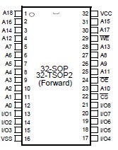
K6T4008V1C-6B70, K6T4008V1C-B, K6T4008V1C-F Selling Leads, Datasheet
MFG:SAMSUNG Package Cooled:SOP D/C:09+

K6T4008V1C-6B70, K6T4008V1C-B, K6T4008V1C-F Datasheet download

Part Number: K6T4008V1C-6B70
MFG: SAMSUNG
Package Cooled: SOP
D/C: 09+


MFG:SAMSUNG Package Cooled:SOP D/C:09+

K6T4008V1C-6B70, K6T4008V1C-B, K6T4008V1C-F Datasheet download

MFG: SAMSUNG
Package Cooled: SOP
D/C: 09+
Want to post a buying lead? If you are not a member yet, please select the specific/related part number first and then fill the quantity and your contact details in the "Request for Quotation Form" on the left, and then click "Send RFQ".Your buying lead can then be posted, and the reliable suppliers will quote via our online message system or other channels soon.
TOP
PDF/DataSheet Download
Datasheet: K6T0808C1D
File Size: 174409 KB
Manufacturer: SAMSUNG [Samsung semiconductor]
Download : Click here to Download
PDF/DataSheet Download
Datasheet: K6T4008V1C-B
File Size: 191385 KB
Manufacturer: SAMSUNG [Samsung semiconductor]
Download : Click here to Download
PDF/DataSheet Download
Datasheet: K6T4008V1C-F
File Size: 191385 KB
Manufacturer: SAMSUNG [Samsung semiconductor]
Download : Click here to Download
The K6T4008V1C and K6T4008U1C families are fabricated by SAMSUNG¢s advanced CMOS process technology. The families support various operating temperature range and have various package type for user flexibility of system design. The families also support low data retention voltage for battery back-up operation with low data retention current.
| Item | Symbol | Ratings | Unit | Remark |
| Voltage on any pin relative to Vss | VIN,VOUT | -0.5 to VCC+0.5 | V | - |
| Voltage on Vcc supply relative to Vss | VCC | -0.3 to 4.6 | V | - |
| Power Dissipation | PD | 1.0 | W | - |
| Storage temperature | TSTG | -65 to 150 | °C | - |
| Operating Temperature | TA | 0 to 70 | °C | K6T4008V1C-L, K6T4008U1C-L |
| -40 to 85 |
°C |
K6T4008V1C-P, K6T4008U1C-P |
1. Stresses greater than those listed under "Absolute Maximum Ratings" may cause permanent damage to the device. Functional operation should be restricted to recommended operating condition. Exposure to absolute maximum rating conditions for extended periods may affect reliability.

