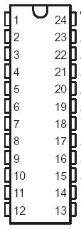
IDT29FCT2052CT, IDT29FCT52, IDT29FCT520 Selling Leads, Datasheet
MFG:IDT Package Cooled:N/A D/C:09+

IDT29FCT2052CT, IDT29FCT52, IDT29FCT520 Datasheet download

Part Number: IDT29FCT2052CT
MFG: IDT
Package Cooled: N/A
D/C: 09+


MFG:IDT Package Cooled:N/A D/C:09+

IDT29FCT2052CT, IDT29FCT52, IDT29FCT520 Datasheet download

MFG: IDT
Package Cooled: N/A
D/C: 09+
Want to post a buying lead? If you are not a member yet, please select the specific/related part number first and then fill the quantity and your contact details in the "Request for Quotation Form" on the left, and then click "Send RFQ".Your buying lead can then be posted, and the reliable suppliers will quote via our online message system or other channels soon.
TOP
PDF/DataSheet Download
Datasheet: IDT29FCT2052CT
File Size: 128669 KB
Manufacturer: IDT [Integrated Device Technology]
Download : Click here to Download
PDF/DataSheet Download
Datasheet: IDT29FCT520A
File Size: 59600 KB
Manufacturer: IDT [Integrated Device Technology]
Download : Click here to Download
PDF/DataSheet Download
Datasheet: IDT29FCT520A
File Size: 59600 KB
Manufacturer: IDT [Integrated Device Technology]
Download : Click here to Download
The IDT29FCT52AT/BT/CT/DT and IDT29FCT53AT/BT/CT are 8-bit registered transceivers built using an advanced dual metal CMOS technology. Two 8-bit back-to-back registers store data flowing in both directions between two bidirectional buses. Separate clock, clock enable and 3-state output enable signals are provided for each register. Both A outputs and B outputs are guaranteed to sink 64mA.
The IDT29FCT52AT/BT/CT/DT and IDT29FCT2052AT/BT/CT are non-inverting options of the IDT29FCT53AT/BT/CT.
The IDT29FCT2052AT/BT/CT has balanced drive outputs with current limiting resistors. This offers low ground bounce,minimal undershoot and controlled output fall times-reducing the need for external series terminating resistors. The IDT29FCT2052T part is a plug-in replacement for IDT29FCT52T part.
| Symbol | Rating | Commercial | Military | Unit |
| VTERM | Terminal Voltage with Respect to GND |
-0.5 to +7.0 | -0.5 to +7.0 | V |
|
VTERM(3) |
Terminal Voltage |
0.5 to |
0.5 to |
V |
| TA | Operating Temperature |
0 to +70 | -55 to +125 | |
| TBIAS | Temperature Under Bias |
-55 to +125 | -65 to +135 | |
| TSTG | Storage Temperature |
-55 to +125 | -65 to +150 | |
|
PT |
Power Dissipation |
0.5 |
0.5 |
W |
| IOUT | DC Output Current |
60 to +120 | 60 to +120 | mA |

