ICX424AL-, ICX424AQ, ICX426AU Selling Leads, Datasheet
MFG:SONY Package Cooled:DIP D/C:N/A

ICX424AL-, ICX424AQ, ICX426AU Datasheet download

Part Number: ICX424AL-
MFG: SONY
Package Cooled: DIP
D/C: N/A


MFG:SONY Package Cooled:DIP D/C:N/A
ICX424AL-, ICX424AQ, ICX426AU Datasheet download
MFG: SONY
Package Cooled: DIP
D/C: N/A

Want to post a buying lead? If you are not a member yet, please select the specific/related part number first and then fill the quantity and your contact details in the "Request for Quotation Form" on the left, and then click "Send RFQ".Your buying lead can then be posted, and the reliable suppliers will quote via our online message system or other channels soon.
TOP
PDF/DataSheet Download
Datasheet: ICX026CKA
File Size: 332459 KB
Manufacturer: SONY [Sony Corporation]
Download : Click here to Download
PDF/DataSheet Download
Datasheet: ICX424AQ
File Size: 261948 KB
Manufacturer: SONY [Sony Corporation]
Download : Click here to Download
PDF/DataSheet Download
Datasheet: ICX026CKA
File Size: 332459 KB
Manufacturer: SONY [Sony Corporation]
Download : Click here to Download
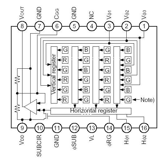
The ICX424AQ is a diagonal 6mm (Type 1/3) interline CCD solid-state image sensor with a square pixel array which supports VGA format. Progressive scan allows all pixels signals to be output independently within approximately 1/60 second. This chip features an electronic shutter with variable charge-storage time which makes it possible to realize full-frame still images without a mechanical shutter. High sensitivity and low dark current are achieved through the adoption of the HAD (Hole-Accumulation Diode) sensors.
This chip is suitable for applications such as FA and surveillance cameras.
| Item | Ratings | Unit | Remarks | |
| Substrate clock SUB GND | 0.3 to +36 | V | ||
| Supply voltage | VDD, VOUT, CGG, SUBCIR GND | 0.3 to +18 | V | |
| VDD, VOUT, CGG, SUBCIR SUB | 22 to +9 | V | ||
| Clock input voltage | V1, V2, V3 GND | 15 to +16 | V | |
| V1, V2, V3 SUB | to +10 | V | ||
| Voltage difference between vertical clock input pins | to +15 | V | ∗2 | |
| Voltage difference between horizongal clock input pins | to +16 | V | ||
| H1, H2 V3 | 16 to +16 | V | ||
| H1, H2 GND | 10 to +15 | V | ||
| H1, H2 SUB | 55 to +10 | V | ||
| VL SUB | 65 to +0.3 | V | ||
| V2, V3 VL | 0.3 to +27.5 | V | ||
| RG GND | 0.3 to +20.5 | V | ||
| V1, H1, H2, GND VL | 0.3 to +17.5 | V | ||
| Storage temperature | 30 to +80 | °C | ||
| Performance guarantee temperature | 10 to +60 | °C | ||
| Operating temperature | 10 to +75 | °C | ||
• Progressive scan allows individual readout of the image signals from all pixels.
• High vertical resolution still images without a mechanical shutter
• Square pixel
• Supports VGA format
• Horizontal drive frequency: 24.54MHz
• No voltage adjustments (reset gate and substrate bias are not adjusted.)
• R, G, B primary color mosaic filters on chip
• High resolution, high color reproductivity, high sensitivity, low dark current
• Continuous variable-speed shutter
• Low smear
• Excellent anti-blooming characteristics
• Horizontal register: 5.0V drive
• 16-pin high precision plastic package (enables dual-surface standard)

Price: 4-6 USD
MT58L64L18CT-10 TQFP100

Price: 5-6.5 USD
DL-7140-211M laser tube

Price: 4-5 USD
74LVC74APG - IC FLIP FLOP D-Type POS-EDG DUAL 14TSSOP

Price: 6.5-8 USD
CYPRESS - Clock Synthesizer with Differential CPU Outputs

Price: 0.284-0.286 USD
PI5V330QEX Pericom Multiplexer Switch ICs

Price: 1-2 USD
IGBT power module, Single switch, 1200 V, Collector-emitter voltage, 430A

Price: 1-2 USD
a-Si TFT-LCD, NEC, 228.096Hmm, 560V

Price: 0.124-0.2 USD
PC354N1T - Mini-flat Package, AC Input Type Photocoupler - Sharp Electrionic Components

Price: 0.177-0.178 USD
RL1210JR51-XX-BL - Thick Film Chip Resistor Low Ohmic - TAITRON Components Incorporated

Price: 0.053-0.055 USD
STPS140A - POWER SCHOTTKY RECTIFIER - STMicroelectronics

Price: 1.45-1.5 USD
STA013 - MPEG 2.5 LAYER III AUDIO DECODER - STMicroelectronics

Price: 0.073-0.075 USD
SMBJ5347B - 5 Watt Surface Mount Silicon Zener Diodes - Micro Commercial Components
