HSTL162822, HSTL162822DGGR, HSTL16918 Selling Leads, Datasheet
Package Cooled:SMD D/C:99

HSTL162822, HSTL162822DGGR, HSTL16918 Datasheet download

Part Number: HSTL162822
MFG: --
Package Cooled: SMD
D/C: 99


Package Cooled:SMD D/C:99

HSTL162822, HSTL162822DGGR, HSTL16918 Datasheet download

MFG: --
Package Cooled: SMD
D/C: 99
Want to post a buying lead? If you are not a member yet, please select the specific/related part number first and then fill the quantity and your contact details in the "Request for Quotation Form" on the left, and then click "Send RFQ".Your buying lead can then be posted, and the reliable suppliers will quote via our online message system or other channels soon.
TOP
PDF/DataSheet Download
Datasheet: HSTL16918
File Size: 94756 KB
Manufacturer:
Download : Click here to Download
PDF/DataSheet Download
Datasheet: HSTL16918
File Size: 94756 KB
Manufacturer:
Download : Click here to Download
PDF/DataSheet Download
Datasheet: HSTL16918
File Size: 94756 KB
Manufacturer:
Download : Click here to Download
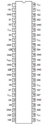
The HSTL16918 is a 9-bit to 18-bit D-type latch designed for 3.15 to 3.45 V VCC operation. The D inputs accept HSTL levels and the Q outputs provide LVTTL levels.
The HSTL16918 is particularly suitable for driving an address bus to two banks of memory. Each bank of nine outputs is controlled with its own latch-enable (LE) input.
Each of the nine D inputs is tied to the inputs of two D-type latches that provide true data (Q) at the outputs. While LE is LOW the Q outputs of the corresponding nine latches follow the D inputs. When LE is taken HIGH, the Q outputs are latched at the levels set up at the D inputs.
The HSTL16918 is characterized for operation from 0 to +70 °C.
|
Symbol |
Parameter |
Cinditions |
Rating |
Unit |
|
VCC |
Supply voltage range |
0.5 to +4.6 |
V | |
|
VI |
Input voltage range 2 | 0.5 to VCC +0.5 | ||
|
VO |
Output voltage range 2 |
0.5 to VCC +0.5 | ||
|
IIK |
Input clamp current | VI < 0 |
-50 |
mA |
|
IOK |
Output clamp current 3 | VO < 0 or VO > VCC |
±50 |
mA |
|
IO |
Continuous output current | VO = 0 to VCC |
±50 |
mA |
| Continuous current through each VCC or GND |
±100 |
mA | ||
|
JA |
Package thermal impedance 4 |
89 |
°C/W | |
|
Tstg |
Storage temperature range |
-65 to 150 |
°C |
NOTES:
1. Stresses beyond those listed may cause permanent damage to the device. These are stress ratings only and functional operation of the device at these or any other conditions beyond those indicated under "recommended operating conditions" is not implied. Exposure to absolute-maximum-rated conditions for extended periods may affect device reliability.
2. The input and output negative-voltage ratings may be exceeded if the input and output clamp-current ratings are observed.
3. This current flows only when the output is in the high state and VO > VCC.
4. The package thermal impedance is calculated in accordance with JESD 51.

