

FDC6401N, FDC640P, FDC6420C Selling Leads, Datasheet
MFG:Fairchild Semiconductor (VA) Category:Discrete Semiconductor Products Package Cooled:SOT163 D/C:04+
FDC6401N, FDC640P, FDC6420C Datasheet download

Part Number: FDC6401N
Category: Discrete Semiconductor Products
MFG: Fairchild Semiconductor (VA)
Package Cooled: SOT163
D/C: 04+
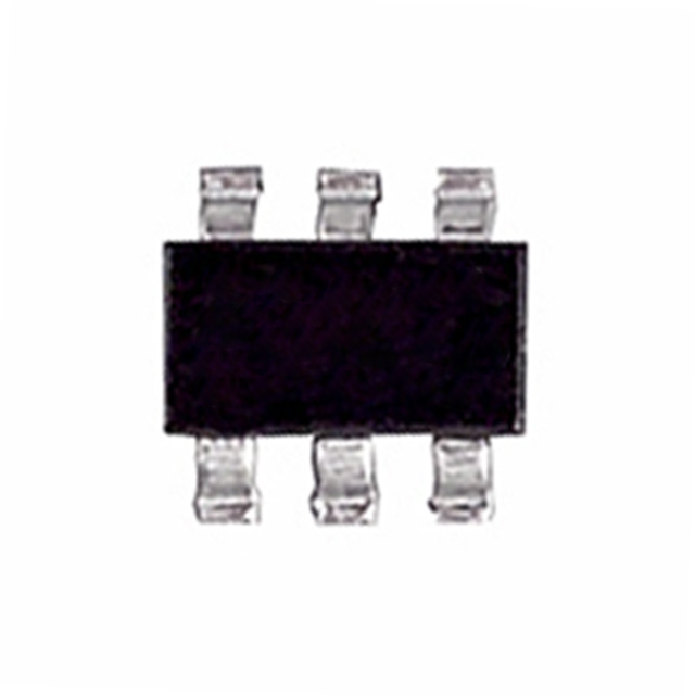
Description: MOSFET N/P-CH 20V 3.0A SSOT-6
Price Break
3000
6000
12000
27000
Unit Price
.13500
.13000
.12800
.12500
Extended Price
405.00
780.00
1536.00
3375.00
(All prices are in USD) Prices for reference only


