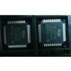
DescriptionThe ZL30102QDG is designed as T1/E1 stratum 4/4E redundant system clock synchronizer which contains a digital phase-locked loop (DPLL). It provides timing and synchronization for DS1/E1 transmission equipment deploying redundant network clocks.ZL30102QDG has fourteen features. (1)Synchr...
ZL30102QDG: DescriptionThe ZL30102QDG is designed as T1/E1 stratum 4/4E redundant system clock synchronizer which contains a digital phase-locked loop (DPLL). It provides timing and synchronization for DS1/E1 t...
SeekIC Buyer Protection PLUS - newly updated for 2013!
268 Transactions
All payment methods are secure and covered by SeekIC Buyer Protection PLUS.
The ZL30102QDG is designed as T1/E1 stratum 4/4E redundant system clock synchronizer which contains a digital phase-locked loop (DPLL). It provides timing and synchronization for DS1/E1 transmission equipment deploying redundant network clocks.
ZL30102QDG has fourteen features. (1)Synchronizes to clock-and-sync-pair to maintain minimal phase skew between an H.110 primary master clock and a secondary master clock. (2)Supports telcordia GR-1244-CORE stratum 4 and 4E. (3)Supports ITU-T G.823 and G.824 for 2048 kbit/s and 1544 kbit/s interfaces. (4)Supports ANSI T1.403 and ETSI ETS 300 011 for ISDN primary rate interfaces. (5)Simple hardware control interface. (6)Manual and Automatic hitless reference switching between any combination of valid input reference frequencies. (7)Accepts three input references and synchronizes to any combination of 8kHz, 1.544MHz, 2.048MHz, 8.192MHz or 16.384 MHz inputs. (8)Provides a range of clock outputs: 1.544MHz, 2.048MHz, 3.088MHz, 6.312MHz, 16.384MHz and either 4.096MHz and 8.192MHz or 32.768MHz and 65.536MHz. (9)Provides 5 styles of 8 kHz framing pulses. (10)Holdover frequency accuracy of 1x10^-7. (11)Provides lock, holdover and selectable out of range indication. (12)Attenuates wander from 1.8Hz. (13)Less than 0.6nspp intrinsic jitter on all output clocks. (14)External master clock source: clock oscillator or crystal. That are all the main features.
Some absolute maximum ratings of ZL30102QDG have been concluded into several points as follow. (1)Its supply voltage would be min -0.5V and max 4.6V. (2)Its core supply voltage would be min -0.5V and max 2.5V. (3)Its voltage on any digital pin would be min -0.5V and max 2.5V. (4)Its voltage on OSCi and OSCo pin would be min -0.3V and max Vdd+0.3V. (5)Its current on any pin would be max 30mA. (6)Its storage temperature range would be min -55°C and max 125°C. (7)Its TQFP 64 pin package power dissipation would be max 500mW. (8)Its ESD rating would be max 2kV. It should be noted that stresses above those listed in absolute maximum ratings may cause permanent damage to device. And so on. If you have any question or suggestion or want to know more information of ZL30102QDG please contact us for details. Thank you!