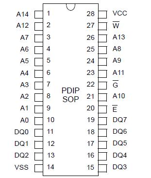
Features: · 32768x8 bit static CMOS RAM· Access times 70 ns, 100 ns· Common data inputs and data outputs· Three-state outputs· Typ. operating supply current 70 ns: 50 mA 100 ns: 40 mA· TTL/CMOS-compatible· Automatical reduction of power dissipation in long Read Cycles· Power supply voltage 5 V + ...
U62256A: Features: · 32768x8 bit static CMOS RAM· Access times 70 ns, 100 ns· Common data inputs and data outputs· Three-state outputs· Typ. operating supply current 70 ns: 50 mA 100 ns: 40 mA· TTL/CMOS-com...
SeekIC Buyer Protection PLUS - newly updated for 2013!
268 Transactions
All payment methods are secure and covered by SeekIC Buyer Protection PLUS.
Features: SpecificationsDescriptionThe U6223B-AFP has the following features including 3-wire-bus ...
Absolute Maximum Ratings a |
Symbol |
Min. |
Max. |
Unit |
Power Supply Voltage |
VCC |
-0.5 |
7 |
V |
Input Voltage |
VI |
-0.5 |
VCC+0.5b |
V |
Output Voltage |
VO |
-0.5 |
VCC+0.5b |
V |
Power Dissipation |
PD |
- |
1 |
W |
Operating Temperature C-Type K-Type A-Type |
Ta |
0 -40 -40 |
70 85 125 |
°C |
Storage Temperature C/K-Type A-Type |
Tstg |
-65 |
125 150 |
°C |
Output Short-Circuit Current at VCC = 5 V and VO = 0 V c |
| IOS | |
200 |
mA |
a Stresses greater than those listed under "Absolute Maximum Ratings" may cause permanent damage to the device. This is a stress rating only,and functional operation of the device at condition above those indicated in the operational sections of this specification is not implied. Exposure to absolute maximum rating conditions for extended periods may affect reliability
b Maximum voltage is 7 V
c Not more than 1 output should be shorted at the same time. Duration of the short circuit should not exceed 30 s.
The U62256A is a static RAM manufactured using a CMOS process technology with the following operating modes:
- Read - Standby
- Write - Data Retention
The memory array is based on a 6-transistor cell.
The U62256A is activated by the falling edge of E. The address and control inputs open simultaneously.According to the information of W and G, the data inputs, or outputs,are active. In a Read cycle, the data outputs are activated by the
falling edge of G, afterwards the data word read will be available at the outputs DQ0-DQ7. After the address change, the data outputs of U62256A go High-Z until the new information read is available. The data outputs have not preferred state.
The Read cycle of U62256A is finished by the falling edge of W, or by the rising edge of E, respectively.Data retention is guaranteed down to 2 V. With the exception of E, all inputs consist of NOR gates, so that no pull-up/pull-down resistors are required.