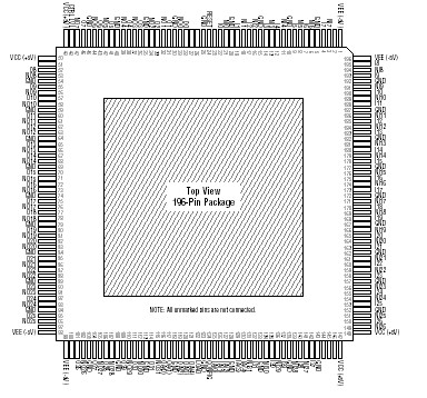
Features: • >25 Gb/s aggregate BW• 800 Mb/s/port NRZ data rate• Non-blocking architecture• 500 ps delay match• Differential ECL-level data I/O; Selectable CMOS/TTLlevel control inputs• Low jitter and signal skew• Fully differential data path• Doub...
TQ8032: Features: • >25 Gb/s aggregate BW• 800 Mb/s/port NRZ data rate• Non-blocking architecture• 500 ps delay match• Differential ECL-level data I/O; Selectable CMOS/TTLle...
SeekIC Buyer Protection PLUS - newly updated for 2013!
268 Transactions
All payment methods are secure and covered by SeekIC Buyer Protection PLUS.
Symbol |
Parameter |
Absolute Max. Rating |
Notes |
TSTOR |
Storage Temperature |
65° C to +150° C |
|
TCH |
Junction (Channel) Temperature |
65° C to +150° C |
1 |
TC |
Case Temperature Under Bias |
65° C to +125° C |
2 |
VCC |
Supply Voltage |
0 V to +7 V |
3 |
VEE |
Supply Voltage |
7 V to 0 V |
3 |
VTT |
Load Termination Supply Voltage |
VEE to 0 V |
4 |
VIN |
Voltage Applied to Any ECL Input; Continuous |
VEE 0.5 V to +0.5 V |
|
IIN |
Current Into Any ECL Input; Continuous |
1.0 mA to +1.0 mA |
|
VIN |
Voltage Applied to Any TTL/CMOS Input; Continuous |
0.5 V to VCC +0.5 V |
|
IIN |
Current Into Any TTL/CMOS Input; Continuous |
1.0 mA to +1.0 mA |
|
VOUT |
Voltage Applied to Any ECL Output |
VEE 0.5 V to +0.5 V |
4 |
IOUT |
Current From Any ECL Output; Continuous |
40 mA |
|
PD |
Power Dissipation per Output POUT = (GND VOUT) x IOUT |
50 mW |
The TQ8032 is a non-blocking 32 x 32 digital crosspoint switch capable of 800 Megabits per second per port data rates. Utilizing a fully differential internal data path and ECL I/O, the TQ8032 offers a high data rate with exceptional signal fidelity. The symmetrical switching and noise rejection characteristics inherent in differential logic result in low jitter and signal skew. The TQ8032 is ideally suited for digital video, data communications and telecommunication switching applications.
The non-blocking architecture of TQ8032 uses 32 fully independent 32:1 multiplexers (see diagram on page 2), allowing each output port to be independently programmed to any input port. The switch is configured by sequentially loading each multiplexer's 5-bit program latch (OA0:4) with the desired input port address (IA0:4) and enabling the LOAD pin. When complete, the CONFIGURE pin of TQ8032 is strobed and all new configurations are simultaneously transferred into the switch multiplexers. Data integrity is maintained on all unchanged data paths.