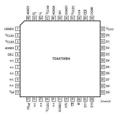
Features: `12-bit resolution`Sampling rate up to 80 MHz` 52 Msps at fIF = 175 MHz; B = 200 kHz (TDA8768BH/5): SFDR = 83 dB, S/N= 71 dB` 80 Msps at fIF = 20 MHz; Nyquist bandwidth (TDA8768BH/8): SFDR = 65 dB, S/N= 62 dB` 80 Msps at fIF = 50 MHz; B = 5 MHz (TDA8768B/8/S1): SFDR = 72 dB, S/N= 64 dB`-...
TDA8768B: Features: `12-bit resolution`Sampling rate up to 80 MHz` 52 Msps at fIF = 175 MHz; B = 200 kHz (TDA8768BH/5): SFDR = 83 dB, S/N= 71 dB` 80 Msps at fIF = 20 MHz; Nyquist bandwidth (TDA8768BH/8): SFDR...
SeekIC Buyer Protection PLUS - newly updated for 2013!
268 Transactions
All payment methods are secure and covered by SeekIC Buyer Protection PLUS.
`12-bit resolution
`Sampling rate up to 80 MHz
` 52 Msps at fIF = 175 MHz; B = 200 kHz (TDA8768BH/5): SFDR = 83 dB, S/N= 71 dB
` 80 Msps at fIF = 20 MHz; Nyquist bandwidth (TDA8768BH/8): SFDR = 65 dB, S/N= 62 dB
` 80 Msps at fIF = 50 MHz; B = 5 MHz (TDA8768B/8/S1): SFDR = 72 dB, S/N= 64 dB
`-3 dB bandwidth of 250 MHz
`5 V power supplies and 3.3 V output power supply
`Binary or twos complement CMOS outputs
`In-range CMOS compatible output
`TTL and CMOS compatible static digital inputs
`TTL and CMOS compatible digital outputs
`Single or Differential clock input; TTL and CMOS compatible
`Power dissipatin 570 mW (typical)
`Low analog input capacitance (typical 2 pF), no buffer amplifier required
`Integrated sample-and-hold amplifier
`Differential analog input
`External amplitude range control
`Voltage controlled regulator included
`-40 to +85 ambient temperature.
SYMBOL | PARAMETER | Conditions | MIN. | MAX. | UNIT |
VCCA | analog supply voltage | [1] | -0.3 | +7.0 | V |
VCCD | digital supply voltage | [1] | -0.3 | +7.0 | V |
VCCO | output stages supply voltage | [1] | -0.3 | +7.0 | V |
VCC | supply voltage difference VCCA - VCCD VCCD - VCCO VCCA - VCCO |
-1.0 -1.0 -1.0 |
+1.0 +4.0 +4.0 |
V | |
VI,VI | input voltage at pins 42 and 43 referenced to AGND |
0.3 | VCCA | V | |
Vclk(p-p) | input voltage at pins 35 and 36 for differential clock drive (peak-to-peak value) |
referenced to AGND | VCCD | V | |
IO | output current | 10 | mA | ||
Tstg | storage temperature | -55 | +150 | ||
Tamb | operating ambient temperature | -40 | +85 | ||
Tj | junction temperature | +150 |
The TDA8768B is a biCMOS 12-bit Analog-to-Digital Converter (ADC) optimized for EDGE and W-CDMA cellular infrastructures, professional telecommunications and other applications such as advanced FM radio and professional imaging. Its main innovation is the RF sampling, based on high-speed clock (up to 80 Msps) combined with a high input frequency (up to 176 MHz). It converts the analog input signal into 12-bit binary coded digital words at a maximum sampling rate of 80 MHz. All static digital inputs (SH, CE and OTC) are TTL and CMOS compatible and all outputs are CMOS compatible. A sine wave clock input signal can also be used.