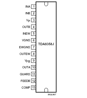
Features: · Few external components required
· High efficiency fully DC-coupled vertical bridge output circuit
· Vertical flyback switch with short rise and fall times
· Built-in guard circuit
· Thermal protection circuit
· Improved EMC performance due to differential inputs
· East-west output stage.Applicationdescribed herein for any of these products are for illustrative purposes only. Philips Semiconductors make no representation or warranty that such applications will be suitable for the specified use without further testing or modification.
Pinout Specifications
|
SYMBOL |
PARAMETER |
CONDITIONS |
MIN. |
MAX. |
UNIT |
|
VP |
supply voltage |
operating |
- |
18 |
V |
|
VFB |
flyback supply voltage |
|
- |
68 |
V |
|
VVGNDEWGND |
voltage difference between
pins VGND and EWGND |
|
- |
0.3 |
V |
|
Vn |
DC voltage
pins OUTA and OUTEW
pin OUTB
pins INA, INB, INEW, GUARD,
FEEDB, and COMP |
note 1 |
-
-
-0.5 |
68
VP
VP |
V
V
V |
|
In |
DC current
pins OUTA and OUTB
pins OUTA and OUTB
pins INA, INB, INEW, GUARD,
FEEDB, and COMP
pin OUTEW |
during scan (p-p)
at flyback (peak); t 1.5 ms |
-
-
-20
- |
3.2
±1.8
+20
750 |
A
A
mA
mA |
|
Ilu |
latch-up current |
input current into any pin;
pin voltage is 1.5 ´ VP; Tj = 150
|
- |
+200 |
mA |
input current out of any pin;
pin voltage is -1.5 ´ VP; Tj = 150 |
-200 |
- |
mA |
|
Ves |
electrostatic handling voltage |
machine model; note 2 |
-350 |
+350 |
V |
| human body model; note 3 |
-4000 |
+4000 |
V |
|
PEW |
east-west power dissipation |
note 4 |
- |
4 |
W |
|
Ptot |
total power dissipation |
|
- |
15 |
W |
|
Tstg |
storage temperature |
|
-55 |
+150 |
|
|
Tamb |
ambient temperature |
|
-25 |
+85 |
|
|
Tj |
junction temperature |
note 5 |
- |
+150 |
|
Notes
1. When the voltage at pin OUTA supersedes 70 V the circuit will limit the voltage.
2. Equivalent to 200 pF capacitance discharge through a 0
resistor.
3. Equivalent to 100 pF capacitance discharge through a 1.5 k
resistor.
4. For repetitive time durations of t < 0.1 ms or a non-repetitive time duration of t < 5 ms the maximum (peak)
east- west power dissipation PEW(peak) = 15 W.
5. Internally limited by thermal protection at T
j » 170.
DescriptionThe TDA8358J is a power circuit for use in 90° and 110° colour deflection systems for 25 to 200 Hz field frequencies, and for 4 : 3 and 16 : 9 picture tubes. The IC contains a vertical deflection output circuit, operating as a high efficiency class G system. The full bridge output TDA8358J circuit allows DC coupling of the deflection coil in combination with single positive supply voltages.
The east-west output stage is able to supply the sink current for a diode modulator circuit.
The TDA8358J is constructed in a Low Voltage DMOS (LVDMOS) process that combines bipolar, CMOS and DMOS devices. DMOS transistors are used in the output stage because of absence of second breakdown.

 TDA8358J Data Sheet


