TDA8354Q

Features: · Few external components required· High efficiency fully DC-coupled vertical output bridge circuit· Vertical flyback switch with short fall and rise times· Built-in guard circuit· Thermal protection circuit· Improved EMC performance due to differential inputs· A guard signal in zoom mod...

product image

TDA8354Q Picture
SeekIC No. : 004516734 Detail

TDA8354Q: Features: · Few external components required· High efficiency fully DC-coupled vertical output bridge circuit· Vertical flyback switch with short fall and rise times· Built-in guard circuit· Thermal...

floor Price/Ceiling Price

Part Number:
TDA8354Q
Supply Ability:
5000

Price Break

  • Qty
  • 1~5000
  • Unit Price
  • Negotiable
  • Processing time
  • 15 Days
Total Cost: $ 0.00

SeekIC Buyer Protection PLUS - newly updated for 2013!

  • Escrow Protection.
  • Guaranteed refunds.
  • Secure payments.
  • Learn more >>

Month Sales

268 Transactions

Rating

evaluate  (4.8 stars)

Upload time: 2025/1/12

Payment Methods

All payment methods are secure and covered by SeekIC Buyer Protection PLUS.

Notice: When you place an order, your payment is made to SeekIC and not to your seller. SeekIC only pays the seller after confirming you have received your order. We will also never share your payment details with your seller.
Product Details

Description


Features:

· Few external components required
· High efficiency fully DC-coupled vertical output bridge circuit
· Vertical flyback switch with short fall and rise times
· Built-in guard circuit
· Thermal protection circuit
· Improved EMC performance due to differential inputs
· A guard signal in zoom mode.


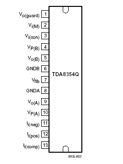
Pinout

  Connection Diagram


Specifications

SYMBOL
PARAMETER
CONDITIONS
MIN.
MAX.
UNIT
DC supply
VP
supply voltage  
-
18
V
Vflb
flyback supply voltage
-
68
V
Vertical circuit
IO(p-p)
output current (peak-to-peak value)
-
3.2
A
VO(A)
output voltage
note 1
-
68
V
Vo(B)
output voltage  
-
VP
V
I1,2,3,11,12,13 current in or out of pins 1 to 3 and 11 to 13  
-20
+20
mA
V1,2,3,11,12,13 peak voltage on pins 1 to 3 and 11 to 13  
-0.5
VP
V
Flyback switch
Io(Vflb)
peak output current t 1.5 ms
-
±1.6
A
Thermal data (in accordance with IEC 60747-1)
Tstg
storage temperature
-55
+150
Tamb
operating ambient temperature
-25
+85
Tvj
virtual junction temperature note 2
-
150
Miscellaneous
tsc
short-circuiting time note 3
-
1
hr
Ii/o
current into any pin 1.5 * VP (ABSmax); note 4
-
+200
mA
current out of any pin -1.5 * VP (ABSmax); note 4
-200
-
mA
VESD
electrostatic handling machine model note 5
-
±300
V
electrostatic handling human body model note 6
-
±2000
V

Notes
1. When the pin voltage exceeds 70 V, the device functions asa power Zener diode, and limits the voltage.
2. Internally limited by thermal protection; switching point » 170 .
3. Up to VP = 18 V.
4. Latch-up test at Tj(max).
5. Machine model: equivalent to discharging a 200 pF capacitor through a 0 series resistor.
6. Human body model: equivalent to discharging a 100 pF capacitor through a 1.5 kseries resistor.


Description

The TDA8354Q is a power circuit for use in 90° and 110° colour deflection systems for 25 to 200 Hz field frequencies, and for 4 : 3 and 16 : 9 picture tubes. The IC contains a vertical deflection output circuit, operating as a high efficiency class G system. The full bridge output circuit allows DC coupling of the deflection coil in combination with single positive supply voltages.

The IC of the TDA8354Q is constructed in a Low Voltage DMOS (LVDMOS) process that combines bipolar, CMOS and DMOS devices. DMOS transistors are used in the output stage because of the absence of second breakdown.


Customers Who Bought This Item Also Bought

Margin,quality,low-cost products with low minimum orders. Secure your online payments with SeekIC Buyer Protection.
Cables, Wires - Management
Line Protection, Backups
Industrial Controls, Meters
Semiconductor Modules
Audio Products
View more