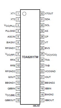
Features: · Direct conversion Quadrature Phase Shift Keying (QPSK) and 8PSK demodulation (Zero-IF)· 950 to 2175 MHz frequency range· High-level asymmetrical RF input· 0 to 50 dB variable gain on RF input· Loop-controlled 0° to 90° phase shifter· High AGC linearity (<1 dB per bit with an 8-bit D...
TDA8261TW: Features: · Direct conversion Quadrature Phase Shift Keying (QPSK) and 8PSK demodulation (Zero-IF)· 950 to 2175 MHz frequency range· High-level asymmetrical RF input· 0 to 50 dB variable gain on RF ...
SeekIC Buyer Protection PLUS - newly updated for 2013!
268 Transactions
All payment methods are secure and covered by SeekIC Buyer Protection PLUS.
The direct conversion QPSK demodulator TDA8261TW is the front-end receiver dedicated to digital TV broadcasting, satisfying both DVB and DBS TV standards. The wide range oscillator (from 950 to 2175 MHz) covers the American, European and Asian satellite bands, as well as the Satellite Master Antennae (SMA) TV US standard.
The Zero-IF concept discards traditional IF filtering and intermediate conversion techniques. It also simplifies the signal path.
TDA8261TW Optimum signal level is guaranteed by gain controlled amplifiers in the RF path. The 0 to 50 dB variable gain is controlled by the signal returned from the Satellite Demodulator and Decoder (SDD) and applied to pin AGCIN.
The PLL synthesizer is built on a dual-loop concept. The first loop controls a fully integrated L-band oscillator, using the LC VCO as a reference which runs at a quarter of the synthesized frequency.
The second loop controls the tuning voltage of the VCO and improves the phase noise of the carrier within the loop bandwidth. The step size is equal to the comparison frequency. The input of the main divider of the PLL synthesizer is connected internally to the VCO output.
The comparison frequency of the second loop is obtained from an oscillator driven by an external 4 MHz crystal. The 4 MHz output available at pin XTOUT may be used to drive the crystal inputs of the SDD, saving an additional crystal in the application.
Both the divided and the comparison frequencies of the TDA8261TW second loop are compared in a fast phase detector which drives the charge pump. The TDA8261TW includes a loop amplifier with an internal high-voltage transistor to drive an
external 33 V tuning voltage.
Control data is entered via the I2C-bus. The I2C-bus voltage can be 5, 3.3 or 2.5 V, allowing compatibility with most of the existing microcontrollers.
A 5-byte frame is required to address the device and to program the main divider ratio, the reference divider ratio, the charge pump current and the operating mode.
A flag is set when the loop is 'in-lock'. This flag can be read during read operations, as well as the Power-On Reset
(POR) flag.
The TDA8261TW has four selectable I2C-bus addresses. The selection is done by applying a specific voltage to pin AS. This feature gives the possibility to use up to four TDA8261TW ICs in the same system.