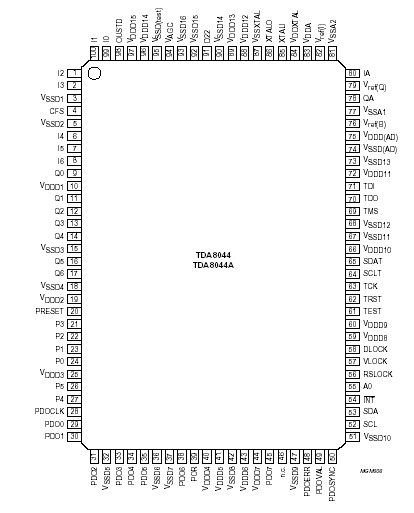
Features: ` General features:
One-chip Digital Video Broadcasting (DVB) compliant Quadrature Phase Shift Keying (QPSK) and Binary
Phase Shift Keying (BPSK) demodulator and concatenated Viterbi/Reed-Solomon decoder with de-
interleaver and de-randomizer (ETS 300 421)
3.3 V supply voltage (input pads are 5 V tolerant)
Standby mode for low power dissipation
Internal clock PLL to allow low frequency crystal application and selectable clock frequencies
Power-on reset module
Package: QFP100
Boundary scan test.
` QPSK/BPSK demodulator:
Interpolator and anti-alias filter to handle a large range of symbol rates without additional external filtering
On-chip AGC of the analog input I and Q baseband signals or tuner AGC control
Two on-chip matched Analog-to-Digital Converters (ADCs; 7 bits)
Half Nyquist (square root raised-cosine) filter with selectable roll-off factor
Large range of symbol frequencies:
0.5 to 45 Msymbols/s for TDA8044 and
0.5 to 30 Msymbols/s for TDA8044A, including Single Carrier Per Channel (SCPC) function
Can be used at low channel Signal-to-Noise ratio (S/N)
Internal carrier recovery, clock recovery and AGC loops with programmable loop filters
Two loop carrier recovery enabling phase tracking of the incoming symbols
Software carrier sweep for low symbol rate applications
Signal-to-noise ratio estimation
External indication of demodulator lock.
` Viterbi decoder:
Rate 1¤2 convolutional code based
Constraint length K = 7 with G1 = 171oct and G2 = 133oct; supported puncturing code rates: 1/2, 2/3, 3/4,
4/5, 5/6, 6/7, 7/8 and 8/9
4 bits input for 'soft decision' for both I and Q
Truncation length: 144
Automatic synchronization
Channel Bit Error Rate (BER) estimation
External indication of Viterbi sync lock
Differential decoding optional.
` Reed-Solomon (RS) decoder:
(204, 188, T = 8) Reed-Solomon code
Automatic (I2C-bus configurable) synchronization of bytes, transport packets and frames
Internal convolutional de-interleaving (I = 12; using internal memory)
De-randomizer based on Pseudo Random Bit Sequence (PRBS)
External indication of Register Select (RS) decoder sync lock
External indication of uncorrectable error (transport error indicator is set)
External indication of corrected byte
Indication of the number of lost blocks
Indication of the number of corrected blocks.
` Interface:
I2C-bus interface to initialize and monitor the demodulator and Forward Error Correction (FEC) decoder;
when no I2C-bus usage, default mode is defined
Programmable interrupt facility
6 bits I/O expander for flexible access to and from the I2C-bus
Switchable I2C-bus loop-through to suppress I2C-bus crosstalk in the tuner
DiSEqC level 1.X support for dish control applications
3-state mode for transport stream outputs.
Application· Digital satellite TV: demodulation and Forward Error Correction (FEC).
Pinout Specifications
|
SYMBOL |
PARAMETER |
CONDITIONS |
MIN. |
MAX. |
UNIT |
|
VDD |
supply voltage pins |
|
-0.3 |
+3.55 |
V |
|
Vmax |
maximum voltage on all pins |
|
0 |
VDD |
V |
|
Ptot |
total power dissipation
TDA8044
TDA8044A |
Tamb = 70; note 1
Tamb = 70; note 2 |
-
- |
1700
1250 |
mW
mW |
|
Tstg |
IC storage temperature |
|
-55 |
+150 |
|
|
Tamb |
ambient temperature |
Tamb = 70 |
0 |
70 |
|
|
Tj |
operating junction temperature |
|
0 |
125 |
|
Notes
1. Maximum power dissipation is specified for 96 MHz clock frequency, 45 Msymbols/s and a puncture rate of 7¤8.
2. Maximum power dissipation is specified for 64 MHz clock frequency, 30 Msymbols/s and a puncture rate of 7¤8.
DescriptionThis document gives preliminary information about the TDA8044 and TDA8044A, which are the successors of the TDA8043. The TDA8044A is only specified where the product deviates from the TDA8044, all other references are the same. The TDA8044 is backwards compatible with the TDA8043, with respect to pinning and the I2C-bus software. The TDA8044 is a DVB compliant demodulator and error correction decoder IC for reception of QPSK and BPSK modulated signals for satellite applications. It can handle variable symbol rates in the range of 0.5 to 45 Msymbols/s (0.5 to 30 Msymbols/s for TDA8044A) with a minimum number of low cost and non-critical external components. Typical applications for this device are Multi Channel Per Carrier (MCPC), Single Channel Per Carrier (SCPC) and simulcast. In these applications one satellite transponder contains respectively one broad QPSK carrier, several small QPSK carriers and one small QPSK carrier together with one or two FM carriers.
The TDA8044 has minimum interface with the tuner, it only requires the demodulated analog I and Q baseband input
signals. Analog-to-digital conversion is performed internally by two matched 7-bit ADCs. Since all the loops (AGC, clock and carrier recovery) are internal, no feedback to the tuner is needed. However, for maximum tuner flexibility, there is the possibility to close the AGC and carrier recovery loop externally via the tuner.
The number of external components required for operation of the TDA8044 is very low. Moreover the external components are low cost and non-critical. This gives an easy and low cost application. The TDA8044 operates on a low frequency crystal which is upconverted to a clock frequency by means of an internal PLL. Different clock frequencies can be selected with the PLL without changing the crystal. This allows for maximum flexibility concerning symbol rate range combined with minimum power consumption.
The TDA8044 also has internal anti-alias filters, which can cover a large range of symbol frequencies (approximately
one decade) without the need to switch external (SAW) filters. To cover the whole range of 0.5 to 45 Msymbols/s
switching of clock frequency (internally) and filtering (externally) is necessary.
The TDA8044 has a double carrier loop configuration which has excellent capabilities of tracking phase noise. Synchronization of the FEC unit is done completely internally, thereby minimizing I2C-bus communication. The output of the TDA8044 is highly flexible, allowing different output modes to interface to a demultiplexer/descrambler/MPEG-2 decoder including a 3-state mode. For evaluation of the TDA8044, demodulator and Viterbi outputs can be made available externally.
Interfacing to the TDA8044 has been extended compared to the TDA8043. Separate resets are available for logic only, logic plus I2C-bus and carrier loops. A Power-on reset module has been implemented which gives a reset signal at power-up. This signal can be used to reset the TDA8044 in order to guarantee correct starting of the IC. Two extra general purpose I/O pins (I/O expanders) have been added. A switchable I2C-bus loop-through to the tuner is implemented to switch-off the I2C-bus connection to the tuner. This reduces phase noise in the tuner in the event of I2C-bus crosstalk. The transport stream outputs can be put in 3-state mode. DiSEqC level 1.X support is integrated for dish control applications. The power consumption in standby mode has been decreased considerably.

 TDA8044 Data Sheet


