QS5919

Features: • 5V operation• Low noise CMOS level outputs• < 500ps output skew, Q0Q4• 2xQ output, Q outputs, Q output, Q/2 output• Outputs 3-state and reset while OE/RST low• PLL disable feature for low frequency testing• Internal loop filter RC network...

product image

QS5919 Picture
SeekIC No. : 004468525 Detail

QS5919: Features: • 5V operation• Low noise CMOS level outputs• < 500ps output skew, Q0Q4• 2xQ output, Q outputs, Q output, Q/2 output• Outputs 3-state and reset while OE/RS...

floor Price/Ceiling Price

Part Number:
QS5919
Supply Ability:
5000

Price Break

  • Qty
  • 1~5000
  • Unit Price
  • Negotiable
  • Processing time
  • 15 Days
Total Cost: $ 0.00

SeekIC Buyer Protection PLUS - newly updated for 2013!

  • Escrow Protection.
  • Guaranteed refunds.
  • Secure payments.
  • Learn more >>

Month Sales

268 Transactions

Rating

evaluate  (4.8 stars)

Upload time: 2024/11/21

Payment Methods

All payment methods are secure and covered by SeekIC Buyer Protection PLUS.

Notice: When you place an order, your payment is made to SeekIC and not to your seller. SeekIC only pays the seller after confirming you have received your order. We will also never share your payment details with your seller.
Product Details

Description


Features:

• 5V operation
• Low noise CMOS level outputs
• < 500ps output skew, Q0Q4
• 2xQ output, Q outputs, Q output, Q/2 output
• Outputs 3-state and reset while OE/RST low
• PLL disable feature for low frequency testing
• Internal loop filter RC network
• Functional equivalent to Motorola MC88915
• Positive or negative edge synchronization (
• Balanced drive outputs ±36mA
• 160MHz maximum frequency (2xQ output)
• Available in QSOP and PLCC packages


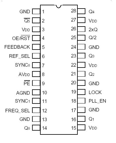
Pinout

  Connection Diagram


Specifications

Symbol
Description
Commercial
& Industrial
Unit
VDDQ, VDD
Supply Voltage to Ground
0.5 to +7
V
VI
DC Input Voltage
0.5 to +7
V
REF Input Voltage
0.5 to +4.6
V
Maximum Power
Dissipation (TA = 85°C)
QSOP
655
mW
PLCC
770
TSTG
Storage Temperature Range
65 to +150
° C

NOTE:
1. Stresses greater than those listed under ABSOLUTE MAXIMUM  RATINGS may cause permanent damage to the device. This is a stress rating only and functional operation of the device at these or any other conditions above those indicated in the operational sections of this specification is not implied. Exposure to absolute maximum rating conditions for extended periods may affect reliability.


Description

The QS5919 Clock Driver uses an internal phase locked loop (PLL) to lock low skew outputs to one of two reference clock inputs. Eight outputs are available: 2xQ, Q0-Q4, Q5, Q/2. Careful layout and design ensure < 500ps skew between the Q0-Q4, and Q/2 outputs. The QS5919 includes an internal RC filter which provides excellent jitter characteristics and eliminates the need for external components. Various combinations of feedback and a divide-by-2 in the VCO path allow applications to be customized for linear VCO operation over a wide range of input SYNC frequencies. The PLL can also be disabled by the PLL_EN signal to allow low frequency or DC testing. The LOCK output asserts to indicate when phase lock has been achieved. The QS5919 is designed for use in highperformance workstations, multi-board computers, networking hardware, and mainframe systems. Several can be used in parallel or scattered throughout a system for guaranteed low skew, system-wide clock distribution networks.

For more information on PLL clock driver products, see Application Note AN-227.


Customers Who Bought This Item Also Bought

Margin,quality,low-cost products with low minimum orders. Secure your online payments with SeekIC Buyer Protection.
Integrated Circuits (ICs)
Cables, Wires
Optoelectronics
Prototyping Products
DE1
Motors, Solenoids, Driver Boards/Modules
View more