PCK2057

Features: • Optimized for clock distribution in DDR (Double Data Rate) SDRAM applications supporting DDR 200/266/300/333• Full DDR solution provided when used with PCK2002P or PCK2002PL, and PCK2022RA• 1-to-10 differential clock distribution• Very low jitter (< 100 ps)&#...

product image

PCK2057 Picture
SeekIC No. : 004456655 Detail

PCK2057: Features: • Optimized for clock distribution in DDR (Double Data Rate) SDRAM applications supporting DDR 200/266/300/333• Full DDR solution provided when used with PCK2002P or PCK2002PL,...

floor Price/Ceiling Price

Part Number:
PCK2057
Supply Ability:
5000

Price Break

  • Qty
  • 1~5000
  • Unit Price
  • Negotiable
  • Processing time
  • 15 Days
Total Cost: $ 0.00

SeekIC Buyer Protection PLUS - newly updated for 2013!

  • Escrow Protection.
  • Guaranteed refunds.
  • Secure payments.
  • Learn more >>

Month Sales

268 Transactions

Rating

evaluate  (4.8 stars)

Upload time: 2025/1/10

Payment Methods

All payment methods are secure and covered by SeekIC Buyer Protection PLUS.

Notice: When you place an order, your payment is made to SeekIC and not to your seller. SeekIC only pays the seller after confirming you have received your order. We will also never share your payment details with your seller.
Product Details

Description


Features:

• Optimized for clock distribution in DDR (Double Data Rate) SDRAM applications supporting DDR 200/266/300/333
• Full DDR solution provided when used with PCK2002P or PCK2002PL, and PCK2022RA
• 1-to-10 differential clock distribution
• Very low jitter (< 100 ps)
• Operation from 2.2 V to 2.7 V AVDD and 2.3 V to 2.7 V VDD
• SSTL_2 interface clock inputs and outputs
• HCSL to SSTL_2 input conversion
• Test mode enables buffers while disabling PLL
• Tolerant of Spread Spectrum input clock
• 3.3 V I2C support with 3.3 V VDDI2C
• 2.5 V I2C support with 2.5 V VDDI2C
• Form, fit, and function compatible with CDCV850


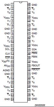
Pinout

  Connection Diagram


Specifications

SYMBOL
PARAMETER
CONDITION
LIMITS
UNIT
MIN
MAX
VDDQ/AVDD
Supply voltage range
0.5
3.6
V
VDDI2C
I2C supply voltage range
0.5
3.6
V
VI
Input voltage range
except SCL and SDA
see Notes 2 and 3
0.5
VDDQ + 0.5
V
SCL and SDA
see Notes 2 and 3
0.5
VDDI2C + 0.5
V
VO
Output voltage range
see Notes 2 and 3
-0.5
VDDQ + 0.5
V
IIK
Input clamp current
VI < 0 or VI >VDDQ
-
±50
mA
IOK
Output clamp current
VO < 0 or VO >VDDQ
-
±50
mA
IO
Continuous output current
VO = 0 to VDDQ
±50
mA
Continuous current to GND or VDDQ
-
±100
mA
Ptot
Storage temperature range
-65
+150
°C
NOTES:
1. Stresses beyond those listed may cause permanent damage to the device. These are stress ratings only and functional operation of the device at these or any other conditions beyond those indicated under "recommended operating conditions" is not implied. Exposure to absolute-maximum-rated conditions for extended periods may affect device reliability.
2. The input and output voltage ratings may be exceeded if the input and output current ratings are observed.
3. This value is limited to 3.6 V maximum.


Description

The PCK2057 is a high-performance, low-skew, low-jitter zero delay buffer that distributes a differential clock input pair (CLK, CLK) to ten differential pairs of clock outputs and one differential pair of feedback clock outputs. The clock outputs are controlled by the clock inputs (CLK, CLK), the feedback clocks (FBIN,FBIN ), the 2-line serial interface (SDA, SCL), and the analog power input (AVDD). The two-line serial interface (I2C) of PCK2057 can put the individual output clock pairs in a high-impedance state. When AVDD is tied to GND, the PLL is turned off and bypassed for test purposes. The PCK2057 provides a standard mode (100 kbits) I2C interface for device control. The implementation is as a slave/receiver. The serial inputs (SDA, SCL) provide integrated pull-up resistors (typically 100 kW).

Two 8-bit, 2-line serial registers of PCK2057 provide individual enable control for each output pair. All outputs default to enabled at power-up. Each output pair can be placed in a high-impedance mode, when a low-level control bit is written to the control register. The registers must be accessed in sequential order (i.e., random access of the registers is not supported). The I2C interface circuit of PCK2057 can be supplied with either 2.5 V or 3.3 V (VDDI2C).

Since the PCK2057 is based on PLL circuitry, it requires a stabilization time to achieve phase-lock of the PLL. This stabilization time is required following power-up.


Customers Who Bought This Item Also Bought

Margin,quality,low-cost products with low minimum orders. Secure your online payments with SeekIC Buyer Protection.
Semiconductor Modules
Sensors, Transducers
Boxes, Enclosures, Racks
Industrial Controls, Meters
Test Equipment
Audio Products
View more