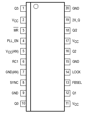
Features: • 2X_Q Output Meets All Requirements of the 20, 25 and 33MHz 68040 Microprocessor PCLK Input Specifications
• 60 and 66MHz Output to Drive the PentiumTM Microprocessor
• Four Outputs (Q0Q3) With OutputOutput Skew <500ps and Six Outputs Total (Q0Q3, 2X_Q) With <1ns
Skew Each Being Phase and Frequency Locked to the SYNC Input
• The Phase Variation From ParttoPart Between SYNC and the 'Q' Outputs Is Less Than 600ps (Derived
From the TPD Specification, Which Defines the ParttoPart Skew)
• SYNC Input Frequency Range From 5MHZ to 2X_Q FMax/4
• Additional Outputs Available at 2X the System 'Q' Frequency
• All Outputs Have ±36mA Drive (Equal High and Low) CMOS Levels. Can Drive Either CMOS or TTL Inputs. All
Inputs Are TTLLevel Compatible
• Test Mode Pin (PLL_EN) Provided for Low Frequency Testing
• Special PowerDown Mode With 2X_Q, Q0, and Q1 Being Reset (With MR), and Other Outputs Remain
Running. 2X_Q, Q0 and Q1 Are Guaranteed to Be in Lock 3 Clock Cycles After MR Is NegatedApplication1. Several specifications can only be measured when the MC88921 is in phaselocked operation. It is not possible
to have the part in phaselock on ATE (automated test equipment). Statistical characterization techniques were
used to guarantee those specifications which cannot be measured on the ATE. MC88921 units were fabricated
with key transistor properties intentionally varied to create a 14 cell designed experimental matrix. IC performance
was characterized over a range of transistor properties (represented by the 14 cells) in excess of the expected
process variation of the wafer fabrication area.
2. A 1M resistor tied to either Analog VCC or Analog GND, as shown in Figure 2, is required to ensure no jitter is
present on the MC88921 outputs. This technique causes a phase offset between the SYNC input and the Q0
output, measured at the pins. The tPD spec describes how this offset varies with process, temperature, and voltage.
The specs were arrived at by measuring the phase relationship for the 14 lots described in note 1 while the part was in phaselocked operation. The actual measurements were made with a 10MHz SYNC input (1.0ns edge rate from 0.8V to 2.0V). The phase measurements were made at 1.5V. See Figure 2 for a graphical description.}
3. Two specs (tRISE/FALL and tPULSE Width 2X_Q output, see AC Specifications) guarantee that the MC88921
meets the 20MHz, 25MHz and 33MHz 68040 PClock input specification (at 40MHz, 50MHz, and 66MHz). For
these two specs to be guaranteed by Motorola, the termination scheme shown in Figure 3 must be used. For
applications which require 1.5V thresholds, but do not require a tight duty cycle the RP resistor can be ignored.
4. The tPD spec (SYNC to Q/2) guarantees how close the Q/2 output will be locked to the reference input connected
to the SYNC input (including temperature and voltage variation). This also tells what the skew from the Q/2
output on one part connected to a given reference input, to the Q/2 output on one or more parts connected to that
reference input (assuming equal delay from the reference input to the SYNC input of each part). Therefore the tPD
spec is equivalent to a parttopart specification. However, to correctly predict the skew from a given output
on one part to any other output on one or more other parts, the distribution of each output in relation to the SYNC
input must be known. This distribution for the MC88921 is provided in Table 1.
Pinout Specifications
|
Symbol |
Parameter |
Value |
Unit |
|
VCC |
DC Supply Voltage (Referenced to GND) |
0.5 to +7.0 |
V |
|
Vin |
DC Input Voltage (Referenced to GND) |
0.5 to VCC +0.5 |
V |
|
Vout |
DC Output Voltage (Referenced to GND) |
0.5 to VCC +0.5 |
V |
|
Iin |
DC Input Current, per Pin |
±20 |
mA |
|
Iout |
DC Output Sink/Source Current, per Pin |
±50 |
mA |
|
ICC |
DC VCC or GND Current per Output Pin |
±50 |
mA |
|
Tstg |
Storage Temperature |
65 to +150 |
|
* Maximum Ratings are those values beyond which damage to the device may occur. Functional operation
should be restricted to the Recommended Operating Conditions.DescriptionThe MC88921 Clock Driver utilizes phaselocked loop technology to lock its low skew outputs' frequency and phase onto an input reference clock. It is designed to provide clock distribution for CISC microprocessor or single processor RISC systems.
The PLL allows the high current, low skew outputs to lock onto a single clock input and distribute MC88921 with essentially zero delay to multiple locations on a board. The PLL also allows the MC88921 to multiply a low frequency input clock and distribute it locally at a higher (2X) system frequency.

 MC88921 Data Sheet


