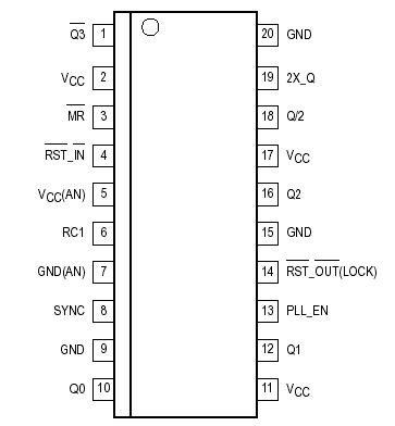
Features: • 2X_Q Output Meets All Requirements of the 20 and 25MHz 68040 Microprocessor PCLK Input Specifications• Three Outputs (Q0Q2) With OutputOutput Skew <500ps and SixOutputs Total (Q0Q2, Q3, 2X_Q,) With <1ns Skew Each Being Phase and Frequency Locked to the SYNC InputR...
MC88920: Features: • 2X_Q Output Meets All Requirements of the 20 and 25MHz 68040 Microprocessor PCLK Input Specifications• Three Outputs (Q0Q2) With OutputOutput Skew <500ps and SixOutputs To...
SeekIC Buyer Protection PLUS - newly updated for 2013!
268 Transactions
All payment methods are secure and covered by SeekIC Buyer Protection PLUS.
1. Several specifications can only be measured when the MC88920 is in phaselocked operation. It is not possible
to have the part in phaselock on ATE (automated test equipment). Statistical characterization techniques were
used to guarantee those specifications which cannot be measured on the ATE. MC88920 units were fabricated
with key transistor properties intentionally varied to create a 14 cell designed experimental matrix. IC performance
was characterized over a range of transistor properties (represented by the 14 cells) in excess of the expected
process variation of the wafer fabrication area. IC performance to each specification and fab variation were
used to set performance limits of ATE testable specifications within those which are to be guaranteed by
statistical characterization. In this way, all units passing the ATE test will meet or exceed the nontested
specifications limits.
2. A 1M resistor tied to either Analog VCC or Analog GND, as shown in Figure 2, is required to ensure no jitter is
present on the MC88920 outputs. This technique causes a phase offset between the SYNC input and the Q0
output, measured at the pins. The tPD spec describes how this offset varies with process, temperature, and voltage.
The specs were arrived at by measuring the phase relationship for the 14 lots described in note 1 while the part was in phaselocked operation. The actual measurements were made with a 10MHz SYNC input (1.0ns edge rate from 0.8V to 2.0V). The phase measurements were made at 1.5V. See Figure 2 for a graphical description.
3. Two specs (tRISE/FALL and tPULSE Width 2X_Q output, see AC Specifications) guarantee that the MC88920
meets the 20MHz and 25MHz 68040 PClock input specification (at 40MHz and 50MHz). For these two specs
to be guaranteed by Motorola, the termination scheme shown in Figure 3 must be used. For applications which
require 1.5V thresholds, but do not require a tight duty cycle the RP resistor can be ignored.
4. The tPD spec (SYNC to Q/2) guarantees how close the Q/2 output will be locked to the reference input connected
to the SYNC input (including temperature and voltage variation). This also tells what the skew from the Q/2 output on one part connected to a given reference input, to the Q/2 output on one or more parts connected to that
reference input (assuming equal delay from the referenceinput to the SYNC input of each part). Therefore the tPD spec is equivalent to a parttopart specification. However, to correctly predict the skew from a given output on one part to any other output on one or more other parts, the distribution of each output in relation to the SYNC input must be known. This distribution for the MC88920 is provided in Table 1.
Symbol |
Parameter |
Value |
Unit |
VCC |
DC Supply Voltage (Referenced to GND) |
0.5 to +7.0 |
V |
Vin |
DC Input Voltage (Referenced to GND) |
0.5 to VCC +0.5 |
V |
Vout |
DC Output Voltage (Referenced to GND) |
0.5 to VCC +0.5 |
V |
Iin |
DC Input Current, per Pin |
±20 |
mA |
Iout |
DC Output Sink/Source Current, per Pin |
±50 |
mA |
ICC |
DC VCC or GND Current per Output Pin |
±50 |
mA |
Tstg |
Storage Temperature |
65 to +150 |
The MC88920 Clock Driver utilizes phaselocked loop technology to lock its low skew outputs' frequency and phase onto an input reference clock. MC88920 is designed to provide clock distribution for CISC microprocessor or single processor RISC systems. The RST_IN/RST_OUT(LOCK) pins provide a processor reset function designed specifically for the
MC68/EC/LC030/040 microprocessor family.
The PLL allows the the high current, low skew outputs to lock onto a single clock input and distribute MC88920 with essentially zero delay to multiple locations on a board. The PLL also allows the MC88920 to multiply a low
frequency input clock and distribute MC88920 locally at a higher (2X) system frequency.