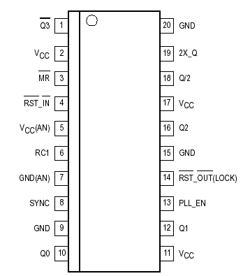
Features: • Provides Performance Required to Drive 68030 Microprocessor Family as well as the 33 and 40MHz 68040 Microprocessors• Three Outputs (Q0Q2) With OutputOutput Skew <500ps and Six Outputs Total (Q0Q2, Q3, 2X_Q,) With <1ns Skew Each Being Phase and Frequency Locked to t...
MC88916: Features: • Provides Performance Required to Drive 68030 Microprocessor Family as well as the 33 and 40MHz 68040 Microprocessors• Three Outputs (Q0Q2) With OutputOutput Skew <500ps a...
SeekIC Buyer Protection PLUS - newly updated for 2013!
268 Transactions
All payment methods are secure and covered by SeekIC Buyer Protection PLUS.
1. Several specifications can only be measured when the MC88916 is in phaselocked operation. It is not possible
to have the part in phaselock on ATE (automated test equipment). Statistical characterization techniques were
used to guarantee those specifications which cannot be measured on the ATE. MC88916 units were fabricated
with key transistor properties intentionally varied to create a 14 cell designed experimental matrix. IC performance
was characterized over a range of transistor properties (represented by the 14 cells) in excess of the expected
process variation of the wafer fabrication area. IC performance to each specification and fab variation were
used to set performance limits of ATE testable specifications within those which are to be guaranteed by
statistical characterization. In this way, all units passing the ATE test will meet or exceed the nontested
specifications limits.
2. A 1M resistor tied to either Analog VCC or Analog GND, as shown in Figure 2, is required to ensure no jitter is
present on the MC88916 outputs. This technique causes a phase offset between the SYNC input and the Q0
output, measured at the pins. The tPD spec describes how this offset varies with process, temperature, and voltage.
The specs were arrived at by measuring the phase relationship for the 14 lots described in note 1 while the
part was in phaselocked operation. The actual measurements were made with a 10MHz SYNC input (1.0ns edge rate from 0.8V to 2.0V). The phase measurements were made at 1.5V. See Figure 2 for a graphical description.
3. The pulse width spec for the Q and 2Q_X outputs is referenced to a VCC/2 threshold. To translate this down to
a 1.5V reference with the same pulse width tolerance, the termination scheme pictured in Figure 3 must be used.
This termination scheme is required to drive the PCLK input of the 68040 microprocessor with the 88916 outputs.
4. The tPD spec (SYNC to Q/2) guarantees how close the Q/2 output will be locked to the reference input connected
to the SYNC input (including temperature and voltage variation). This also tells what the skew from the Q/2 output on one part connected to a given reference input, to the Q/2 output on one or more parts connected to that
reference input (assuming equal delay from the reference input to the SYNC input of each part). Therefore the tPD
spec is equivalent to a parttopart specification. However, to correctly predict the skew from a given output
on one part to any other output on one or more other parts, the distribution of each output in relation to the SYNC
input must be known. This distribution for the MC88916 is
provided in Table 1.
Symbol |
Parameter |
Value |
Unit |
VCC |
DC Supply Voltage (Referenced to GND) |
0.5 to +7.0 |
V |
Vin |
DC Input Voltage (Referenced to GND) |
0.5 to VCC +0.5 |
V |
Vout |
DC Output Voltage (Referenced to GND) |
0.5 to VCC +0.5 |
V |
Iin |
DC Input Current, per Pin |
±20 |
mA |
Iout |
DC Output Sink/Source Current, per Pin |
±50 |
mA |
ICC |
DC VCC or GND Current per Output Pin |
±50 |
mA |
Tstg |
Storage Temperature |
65 to +150 |
The MC88916 Clock Driver utilizes phaselocked loop technology to lock its low skew outputs' frequency and phase onto an input reference clock. It is designed to provide clock distribution for CISC microprocessor or single processor RISC systems. TheRST_IN/RST_OUT(LOCK) pins provide a processor reset function designed specifically for the
MC68/EC/LC030/040 microprocessor family. The 88916 comes in two speed grades: 70 and 80MHz. These frequencies correspond to the 2X_Q maximum output frequency. The two grades should be ordered as the MC88916DW70 and MC88916DW80, respectively.