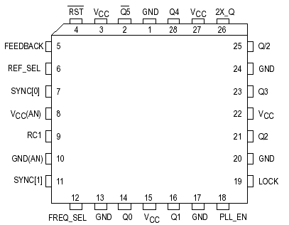
Features: • Five Outputs (QOQ4) with OutputOutput Skew < 500 ps each being phase and frequency locked to the SYNC input• The phase variation from parttopart between the SYNC and FEEDBACK inputs is less than 550 ps (derived from the tPD specification, which defines the parttopart ske...
MC88915: Features: • Five Outputs (QOQ4) with OutputOutput Skew < 500 ps each being phase and frequency locked to the SYNC input• The phase variation from parttopart between the SYNC and FEEDB...
SeekIC Buyer Protection PLUS - newly updated for 2013!
268 Transactions
All payment methods are secure and covered by SeekIC Buyer Protection PLUS.
The MC88915 Clock Driver utilizes phaselocked loop technology to lock its low skew outputs' frequency and phase
onto an input reference clock. It is designed to provide clock distribution for high performance PC's and workstations.
The PLL allows the high current, low skew outputs to lock onto a single clock input and distribute MC88915 with essentially zero delay to multiple components on a board. The PLL also allows the MC88915 to multiply a low frequency input clock and distribute it locally at a higher (2X) system frequency. Multiple 88915's can lock onto a single reference clock, which is ideal for applications when a central system clock must be distributed synchronously to multiple boards (see Figure 7).
Five "Q" outputs (QOQ4) MC88915 are provided with less than 500 ps skew between their rising edges. The Q5 output is inverted (180° phase shift) from the "Q" outputs. The 2X_Q output runs at twice the "Q" output frequency, while the Q/2 runs at 1/2 the "Q" frequency.
The VCO is designed to run optimally between 20 MHz and the 2X_Q Fmax specification. The wiring diagrams in Figure 5 detail the different feedback configurations and the MC88915 create specific input/output frequency relationships. Possible
frequency ratios of the "Q" outputs to the SYNC input are 2:1, 1:1, and 1:2.
The FREQ_SEL pin provides one bit programmable divideby in the feedback path of the PLL. MC88915 selects between
divideby1 and divideby2 of the VCO before its signal reaches the internal clock distribution section of the chip (see the block diagram on page 2). In most applications FREQ_SEL should be held high (÷1). If a low frequency
reference clock input is used, holding FREQ_SEL low (÷2) will allow the VCO to run in its optimal range (>20 MHz).
In normal phaselocked operation the PLL_EN pin is held high. Pulling the PLL_EN pin low disables the VCO and puts
the 88915 in a static "test mode". In MC88915 there is no frequency limitation on the input clock, which is necessary for a low frequency board test environment. The second SYNC input can be used as a test clock input of MC88915 to further simplify boardlevel testing (see detailed description on page 11).
A lock indicator output (LOCK) will go high when the loop is in steadystate phase and frequency lock. The LOCK output of MC88915 will go low if phaselock of MC88915 is lost or when the PLL_EN pin is low. Under certain conditions the lock output may remain low, even though the part is phaselocked. Therefore the LOCK output signal should not be used to drive any active circuitry; it should be used for passive monitoring or evaluation purposes only.