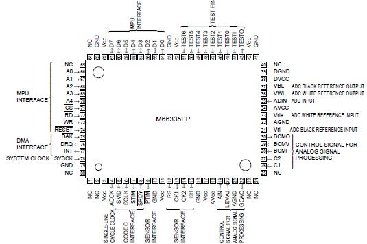
Features: • High speed scan (max. 2 ms/line, typ. 5 ms/line)
• Compatibility with up to the B4 (8 pixels/mm, 16 pixels/mm) image sensor
• Generation of control signals for the image sensor (CCD, CIS)
For CCD: SH, CK1, CK2, RS
For the contact sensor (CIS): SH, CK1, CK2
• Built-in analog processing circuit (equivalent to the M64291)
Sample and hold circuit
Gain control circuit
Black level clamping circuit
Reference internal power supply for the A/D converter
• Built-in A/D converter of a 7-bit flash type
• Built-in image processing memories
Uniformity correction memory, Line memory, Error memory,y correction memory
• External output interface for converted binary data
Serial output (® M66330)
DMA output
• External output interface for multivalued data
DMA transfer of data compensated for uniformity
• Various image processing functions
Uniformity correction
Resolution change from 50% to 200% (by the 1% step)
MTF compensation (2-dimensional processing, capable of correction
for each character/photo)
y correction (capable of correction for each character/photo)
Detection of background/character levels
Change to pseudo-halftone
- Error diffusion (64 tone steps through 6-bit processing)
- Organized dither (64 tone steps through the 8 × 8 matrix)
Image zone separation (2-dimensional processing)
• 5V single power supply
ApplicationFacsimile, word processor and image scannerPinout Specifications
|
Symbol |
Parameter |
Conditions |
Ratings |
Unit |
| VCC |
Supply voltage |
|
0.3 ~ +6.5 |
V |
| VI |
Input voltage |
|
0.3 ~ VCC+0.3 |
V |
| VO |
Output voltage |
|
0 ~ VCC |
V |
| AVCC |
Analog supply voltage |
|
VCC0.3 ~ VCC +0.3 |
V |
| DVCC |
Supply voltage |
|
VCC0.3 ~ VCC +0.3 |
V |
| VWL |
Reference voltage (white) |
|
0.3 ~ AVCC +0.3 |
V |
| VBL |
Reference voltage (black) |
|
0.3 ~ AVCC +0.3 |
V |
| VAIN |
Analog input voltage |
|
0.3 ~ AVCC +0.3 |
V |
| Tstg |
Storage temperature |
|
55 ~ +150 |
|
DescriptionThe M66335 is a facsimile image processing controller to turn into binary signals analog signals which have been output through photoelectric conversion by the image sensor.
The image processing functions includes peak value detection,uniformity correction, resolution change, MTF compensation, y correction,detection of background/character levels, error diffusion,separation of image zones, and designation of regions.
This controller of M66335 contains not only the analog processing circuit, the A/D converter of a 7-bit flash type and image processing memory, but also the image sensor and the interface circuit to the CODEC (Coder and Decoder). Therefore, this LSI alone is capable of image processing.

 M66335FP Data Sheet


