M5M4V16169DTP-8

Features: # 70-pin,400-mil TSOP (type II ) with 0.65mm lead pitch and 23.49mm package length.# Multiplexed DRAM address inputs for reduced pin count and higher system densities.# Selectable output operation (transparent / latched / registered) using set command register cycle.# Single 3.3V +/- 0.3...

product image

M5M4V16169DTP-8 Picture
SeekIC No. : 004406215 Detail

M5M4V16169DTP-8: Features: # 70-pin,400-mil TSOP (type II ) with 0.65mm lead pitch and 23.49mm package length.# Multiplexed DRAM address inputs for reduced pin count and higher system densities.# Selectable output o...

floor Price/Ceiling Price

Part Number:
M5M4V16169DTP-8
Supply Ability:
5000

Price Break

  • Qty
  • 1~5000
  • Unit Price
  • Negotiable
  • Processing time
  • 15 Days
Total Cost: $ 0.00

SeekIC Buyer Protection PLUS - newly updated for 2013!

  • Escrow Protection.
  • Guaranteed refunds.
  • Secure payments.
  • Learn more >>

Month Sales

268 Transactions

Rating

evaluate  (4.8 stars)

Upload time: 2024/11/27

Payment Methods

All payment methods are secure and covered by SeekIC Buyer Protection PLUS.

Notice: When you place an order, your payment is made to SeekIC and not to your seller. SeekIC only pays the seller after confirming you have received your order. We will also never share your payment details with your seller.
Product Details

Description


Features:

# 70-pin,400-mil TSOP (type II ) with 0.65mm lead pitch and 23.49mm package length.
# Multiplexed DRAM address inputs for reduced pin count and higher system densities.
# Selectable output operation (transparent / latched / registered) using set command register cycle.
# Single 3.3V +/- 0.3V Power Supply. (3.3V +/- 0.15V for -7 part)
# 2048 refresh cycles every 64ms (Ad0->Ad10).
# Programmable burst length (1,2,4,8) and burst sequence (sequential,interleave) with no latency.
# Synchronous design for precise control with an external clock (K).
# Output retention by advanced mask clock (CMs#).
# All inputs/outputs low capacitance and LVTTL compatible.
# Separate DRAM and SRAM address inputs for fast SRAM access.
# Page Mode capability.
# Auto Refresh capability.
# Self Refresh capability.


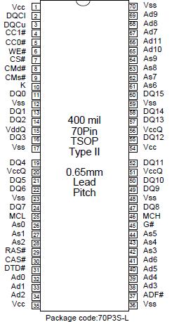
Pinout

  Connection Diagram


Specifications

Symbol
Parameter
Conditions
Ratings
Unit
Vcc
Supply Voltage

With respect to Vss

-0.5 ~ 4.6
V
VI
Input Voltage


-0.5 ~ 4.6
V
VO
Output Voltage


-0.5 ~ 4.6
V
IO
Output Current


50
mA
Pd
Power Dissipation


1000
mW
Topr
Operating Temperature


0 ~ 70
°C
Tstg
Storage Temperature


-65 ~ 150
°C


Description

The M5M4V16169DTP/RT is a 16M-bit Cached DRAM which integrates input registers, a 1,048,576-word by 16-bit dynamic memory array and a 1024- word by 16-bit static RAM array as a Cache memory (block size 8x16) onto a single monolithic circuit. The block data transfer between the DRAM and the data transfer buffers (RB1/RB2/WB1/WB2) is performed in one instruction cycle, a fundamental advantage over a conventional DRAM/SRAM cache.

The M5M4V16169DTP/RT RAM is fabricated with a high performance CMOS process, and is ideal for large-capacity memory systems where high speed, low power dissipation, and low cost are essential. The use of quadruple-layer polysilicon process combined with silicide and double layer aluminum wiring technology, a single-transistor dynamic storage stacked capacitor cell, and a six-transistor static storage cache cell provide high circuit density at reduced costs.


Customers Who Bought This Item Also Bought

Margin,quality,low-cost products with low minimum orders. Secure your online payments with SeekIC Buyer Protection.
Boxes, Enclosures, Racks
Isolators
Computers, Office - Components, Accessories
RF and RFID
Power Supplies - Board Mount
Undefined Category
View more