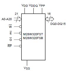
Features: SUPPLY VOLTAGE VDD = 2.7V to 3.6V Core Power Supply VDDQ= 1.65V to 3.6V for Input/Output VPP = 12V for fast Program (optional) ACCESS TIME: 70ns PROGRAMMING TIME: 10s typical Double Word Programming Option Quadruple Word Programming Option COMMON FLASH INTERFACE MEMORY BLOCKS Par...
M28W320FST: Features: SUPPLY VOLTAGE VDD = 2.7V to 3.6V Core Power Supply VDDQ= 1.65V to 3.6V for Input/Output VPP = 12V for fast Program (optional) ACCESS TIME: 70ns PROGRAMMING TIME: 10s typical Double ...
SeekIC Buyer Protection PLUS - newly updated for 2013!
268 Transactions
All payment methods are secure and covered by SeekIC Buyer Protection PLUS.
Symbol |
Parameter |
Value |
Unit | |
Min |
Max | |||
TA |
Ambient Operating Temperature (1) |
40 |
85 |
°C |
TBIAS |
Temperature Under Bias |
40 |
125 |
°C |
TSTG |
Storage Temperature |
55 |
155 |
°C |
VIO |
Input or Output Voltage |
0.6 |
VDDQ +0.6 |
V |
VDD,VDDF |
Supply Voltage |
0.6 |
4.1 |
V |
VPP |
Program Voltage |
0.6 |
13 |
V |
The M28W320FS and M28W640FS are 32 Mbit (2Mbit x 16) and 64 Mbit (4Mbit x 16) Secure Flash memories. The devices can be erased electrically at block level and programmed in-system on a Word-by-Word basis using a 2.7V to 3.6V VDD supply for the circuitry and a 1.65V to 3.6V VDDQ supply for the Input/Output pins. An optional 12V VPP power supply is provided to speed up customer programming.
The M28W320FS and M28W640FS feature 32Mbit and 64 Mbits respectively and have an asymmetrical block architecture with 4 KWord Parameter Blocks and 32 KWord Main Blocks. The M28W320FST and M28W640FST have the Parameter Blocks at the top of the memory address space while the M28W320FSB and M28W640FSB locate the Parameter Blocks starting from the bottom. Refer to Table 1., Figure 5. and Figure 6. for a detailed description of the devices memory architecture and map.
All devices are equipped with hardware and software block protection features to avoid unwanted program/erase (modify) or read of the Flash memory content:
Hardware Protection:
When VPP VPPLK all blocks are protected against program or erase.
Software Protection thanks to KRYPTO Security Features:
Modify Protection: volatile and nonvolatile. Read Protection.
The KRYPTO Security features are described in a dedicated Application Note. Please contact STMicroelectronics for further details. Two registers are available for protection purpose:
The Protection Register
The KRYPTO Protection Register.
The Protection Register of M28W320FS is a 192 bit Protection Register to increase the protection of a system design. The Protection Register is divided into a 64 bit segment and a 128 bit segment. The 64 bit segment contains a unique device number written by ST, while the second one is one-time-programmable by the user. The user programmable segment can be permanently protected. Figure 7., shows the Protection Register Memory Map.
The KRYPTO Protection Register of M28W320FS is used to manage the Modify and Read protection modes. It also features a Device Authentication mechanism. The KRYPTO Protection Register is described in a dedicated Application Note. Please contact STMicroelectronics for further details.
Each block can be erased separately. Erase can be suspended in order to perform either read or program in any other block and then resumed. Program can be suspended to read data in any other block and then resumed. Each block can be programmed and erased over 100,000 cycles. Program and Erase commands are written to the Command Interface of the memory. An on-chip Program/Erase Controller takes care of the timings necessary for program and erase operations.
The end of a program or erase operation can be detected and any error conditions identified. The command set required to control the memory is consistent with JEDEC standards. All the devices are offered in a TBGA64 (10 x 13mm) package.
In order to meet environmental requirements, ST offers the M28W320FS and M28W640FS in ECOPACK® packages. ECOPACK packages are Lead-free. The category of second Level Interconnect is marked on the package and on the inner box label, in compliance with JEDEC Standard JESD97. The maximum ratings related to soldering conditions are also marked on the inner box label.
ECOPACK is an ST trademark. ECOPACK specifications are available at: www.st.com.
All devices are supplied with all the bits erased (set to '1').