LH28F040SUTD-Z4

Features: • 512K * 8 Bit Configuration• 5 V Write/Erase Operation (5 V VPP, 3.3 VCC) VCC for Write/Erase at as low as 2.9 V• Min. 2.7 V Read Capability 190 ns Maximum Access Time (VCC = 2.7 V)• 2 Banks Enable the Simultaneous Read/Write/Erase Operation• 32 Independent...

product image

LH28F040SUTD-Z4 Picture
SeekIC No. : 004394136 Detail

LH28F040SUTD-Z4: Features: • 512K * 8 Bit Configuration• 5 V Write/Erase Operation (5 V VPP, 3.3 VCC) VCC for Write/Erase at as low as 2.9 V• Min. 2.7 V Read Capability 190 ns Maximum Access Time (...

floor Price/Ceiling Price

Part Number:
LH28F040SUTD-Z4
Supply Ability:
5000

Price Break

  • Qty
  • 1~5000
  • Unit Price
  • Negotiable
  • Processing time
  • 15 Days
Total Cost: $ 0.00

SeekIC Buyer Protection PLUS - newly updated for 2013!

  • Escrow Protection.
  • Guaranteed refunds.
  • Secure payments.
  • Learn more >>

Month Sales

268 Transactions

Rating

evaluate  (4.8 stars)

Upload time: 2024/12/25

Payment Methods

All payment methods are secure and covered by SeekIC Buyer Protection PLUS.

Notice: When you place an order, your payment is made to SeekIC and not to your seller. SeekIC only pays the seller after confirming you have received your order. We will also never share your payment details with your seller.
Product Details

Description


Features:

• 512K * 8 Bit Configuration
• 5 V Write/Erase Operation (5 V VPP, 3.3 VCC)
VCC for Write/Erase at as low as 2.9 V
• Min. 2.7 V Read Capability
190 ns Maximum Access Time (VCC = 2.7 V)
• 2 Banks Enable the Simultaneous Read/Write/Erase Operation
• 32 Independently Lockable Blocks (16K)
• 100,000 Erase Cycles per Block
• Automated Byte Write/Block Erase
Command User Interface
Status Register
• System Performance Enhancement
Erase Suspend for Read
Two-Byte Write
Bank Erase
• Data Protection
Hardware Erase/Write Lockout during Power Transitions
Software Erase/Write Lockout
• Independently Lockable for Write/Erase on Each Block (Lock Block and Protect Set/Reset)
• 20 A (Maximum) ICC in CMOS Standby
• State-of-the-Art 0.55 m ETOX™ Flash Technology
• 40-Pin, 1.2 mm * 10 mm * 20 mm TSOP (Type I) Package


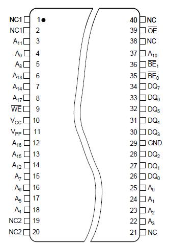
Pinout

  Connection Diagram


Specifications

Temperature under bias ...................... -20 to +80
Storage temperature ......................... -65 to +125
*WARNING: Stressing the device beyond the "Absolute Maximum Ratings" may cause permanent damage. These are stress ratings only. Operation beyond the "Operating Conditions" is not recommended and extended exposure beyond the "Operating Conditions"may affect device reliability.


Customers Who Bought This Item Also Bought

Margin,quality,low-cost products with low minimum orders. Secure your online payments with SeekIC Buyer Protection.
Prototyping Products
DE1
Connectors, Interconnects
Power Supplies - Board Mount
Memory Cards, Modules
Cables, Wires
View more