Features: • User-Configurable x8 or x16 Operation• User-Selectable 3.3 V or 5 V VCC• 70 ns Maximum Access Time• 0.32 MB/sec Write Transfer Rate• 100,000 Erase Cycles per Block• 32 Independently Lockable Blocks• 5 V Write/Erase Operation (5 V VPP) No Requir...
LH28F016SU: Features: • User-Configurable x8 or x16 Operation• User-Selectable 3.3 V or 5 V VCC• 70 ns Maximum Access Time• 0.32 MB/sec Write Transfer Rate• 100,000 Erase Cycles pe...
SeekIC Buyer Protection PLUS - newly updated for 2013!
268 Transactions
All payment methods are secure and covered by SeekIC Buyer Protection PLUS.
Features: • 512K * 8 Word Configuration• 5 V Write/Erase Operation (5 V VPP, 3.3 V VCC...
Features: • 512K * 8 Word Configuration• 5 V Write/Erase Operation (5 V VPP) No Requir...
• User-Configurable x8 or x16 Operation
• User-Selectable 3.3 V or 5 V VCC
• 70 ns Maximum Access Time
• 0.32 MB/sec Write Transfer Rate
• 100,000 Erase Cycles per Block
• 32 Independently Lockable Blocks
• 5 V Write/Erase Operation (5 V VPP)
No Requirement for DC/DC Converter to Write/Erase
• Minimum 2.7 V Read capability
160 ns Maximum Access Time (VCC = 2.7 V)
• Revolutionary Architecture
Pipelined Command Execution
Write During Erase
Command Superset of Sharp LH28F008SA
• 5 A (Typ.) ICC in CMOS Standby
• 1 A (Typ.) Deep Power-Down
• State-of-the-Art 0.55 m ETOX™ Flash Technology
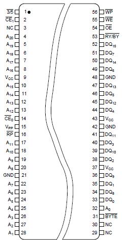
• 56-Pin, 1.2 mm * 14 mm * 20 mm TSOP (Type I) Package
Temperature under bias ......................... 0 to +80
Storage temperature ......................... -65 to +125
*WARNING: Stressing the device beyond the "Absolute Maximum Ratings" may cause permanent damage. These are stress ratings only. Operation beyond the "Operating Conditions" is not recommended and extended exposure beyond the "Operating Conditions"may affect device reliability.
The LH28F016SU is a high performance 16M (16,777,216 bit) block erasable non-volatile random access memory organized as either 1M × 16 or 2M × 8.
The LH28F016SU includes thirty-two 64K (65,536) blocks or thirty-two 32-KW (32,768) blocks. A chip memory map is shown in Figure 4.
The implementation of a new architecture, with many enhanced features, will improve the device operating characteristics and results in greater product reliability and ease of use.
Among the significant enhancements of the LH28F016SU:
• 5 V Write/Erase Operation (5 V VPP)
• 3.3 V Low Power Capability (2.7 V VCC Read)
• Improved Write Performance
• Dedicated Block Write/Erase Protection
A 3/5 input pin reconfigures the device internally for optimized 3.3 V or 5.0 V read/write operation.
The LH28F016SU will be available in a 56-pin, 1.2 mm thick × 14 mm × 20 mm TSOP (Type I) package. This form factor and pinout allow for very high board layout densities.