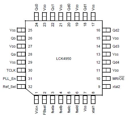
Features: Fully integrated phase-locked loop (PLL) Oscillator or crystal reference input Output frequency up to 180 MHz Outputs disable in high impedance Compatible with PowerPC®, Intel®, and highperformance RISC microprocessors TQFP packaging Output frequency configurable ±35 ps typical ...
LCK4950: Features: Fully integrated phase-locked loop (PLL) Oscillator or crystal reference input Output frequency up to 180 MHz Outputs disable in high impedance Compatible with PowerPC®, Intel®, a...
SeekIC Buyer Protection PLUS - newly updated for 2013!
268 Transactions
All payment methods are secure and covered by SeekIC Buyer Protection PLUS.
Parameter |
Symbol |
Min |
Max |
Unit |
Supply Voltage |
VDD, VDDA |
0.3 |
4.6 |
V |
Input Voltage |
VI |
0.3 |
VDD + 0.3 |
V |
Input Current |
IIN |
- |
±20 |
mA |
Storage Temperature Range |
TStor |
40 |
125 |
°C |
The LCK4950 is a PLL-based clock driver device intended for high-performance clock tree designs.
The LCK4950 is 3.3 V compatible with output frequencies of up to 180 MHz and output skews of 200 ps. The LCK4950 can accommodate the most demanding tree designs by employing a fully differential PLL design. This minimizes cycle-to-cycle jitter, which is critical when the device is acting as the reference clock for PLLs in today's microprocessors and ASICs. The device has nine low-skew configurable outputs for support of the clocking needs of the various high-performance microprocessors.
To provide input reference clock flexibility, two selectable division ratios are available on the LCK4950. The internal VCO runs at either 2x or 4x the high-speed output. The FBSEL pin is used to select between a divide by 8 or a divide by 16 of the VCO frequency to be compared with the input reference. These selections allow the input reference to be either one-half, one-fourth, or one-eighth of the high-speed output.
The LCK4950 is capable of scan clock distribution or system diagnostics due to an external test clock input. The REF_SEL pin allows the selection between a crystal input to an on-chip oscillator for the reference or selection of a TTL level oscillator input directly. Only a parallel resonant crystal is required for the onboard crystal oscillator external components.
The LCK4950 is fully 3.3 V compatible and requires no external loop filter components. All inputs accept LVCMOS or LVTTL compatible levels while the outputs provide LVCMOS levels with the capability to drive terminated 50 transmission lines. The LCK4950 can drive two traces, giving the device an effective fan out of 1:18 for series-terminated 50 lines. For optimum performance and board density, the device is packaged in a 7 mm x 7 mm 32-lead TQFP package.