Features: ` Output operating frequencies up to 1.25 GHz max.
` 100 ps parttopart skew.
` 40 ps typical outputtooutput skew.
` Cycle-to-cycle jitter 5 ps max.
` 3.3 V and 2.5 V compatible.
` Internal input pulldown resistors.
` Q output will default low with inputs open or at VEE.
` Meets or exceeds Joint Electron Device Engineering Council (JEDEC) specification EIA®/JESD78 IC latchup test.
` Moisture sensitivity level 1.
` Flammability rating: UL®94 code V0 at 1/8 in., oxygen index 28 to 34.
` Pin-for-pin compatible with ON Semiconductor® part number MC100LVE310.Pinout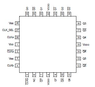 Specifications
Stresses which exceed the absolute maximum ratings can cause permanent damage to the device. These are absolute stress ratings only. Functional operation of the device is not implied at these or any other conditions in excess of those given in the operational sections of the data sheet. Exposure to absolute maximum ratings for extended periods of time can adversely affect device reliability.
| Parameter |
Symbol |
Conditions |
Min |
Max |
Unit |
| PECL Mode Positive Power Supply |
VDD |
VEE = 0 V |
0 |
5 |
V |
Input Voltage:
PECL Mode Positive Input Voltage |
VI
|
VEE = 0 V, VI VDD
|
0 |
15 |
V |
| Output Current |
IOUT |
Continuous surge |
50 |
100 |
mA |
| VBB Sink/Source |
IBB |
- |
-0.5 |
0.5 |
mA |
| Storage Temperature Range |
Tstg |
- |
-65 |
150 |
|
| Wave Solder |
TSOL |
<2 s to 3 s at 248 °C |
- |
265 |
|
DescriptionThe LCK4310 is a low-voltage, low-skew 2:8 differential emitter-coupled logic (ECL) fanout buffer designed with clock distribution in mind. The device features fully differential clock paths to minimize both device and system skew. The LCK4310 offers two selectable clock inputs to allow for redundant or test clocks to be incorporated into the system clock trees.
To ensure that the tight skew specification is met, it is necessary that both sides of the differential output are terminated into 50 , even if only one side is being used. In most applications, all eight differential pairs will be used and therefore terminated. In the case where fewer than eight pairs are used and in order to maintain minimum skew, it is necessary to terminate at least the output pairs adjacent to the output pair being used. Failure to follow this guideline will result in small degradations of propagation delay (on the order of 10 ps-20 ps) of the outputs being used. While not catastrophic to most designs, this will result in an increase in skew.
Note: The package corners isolate outputs from one another such that the guideline expressed above holds only for outputs on the same side of the package.
The LCK4310, as with most ECL devices, can be operated from a positive voltage supply (VDD) in LVPECL mode. This allows the LCK4310 to be used for high-performance clock distribution in 3.3 V/2.5 V systems. Designers can take advantage of the LCK4310's performance to distribute lowskew clocks across the backplane or the board. In a PECL environment (series or Thevenin), line terminations are typically used since they require no additional power supplies. If parallel termination is desired, a terminating voltage of VDD 2.0 V will need to be provided.
An internally generated voltage supply (VBB pin) is available to this device only. For single-ended input conditions, the unused differential input is connected to VBB as a switching reference voltage. VBB may also rebias ac coupled inputs. When used, decouple VBB and VDD via a 0.01 F capacitor and limit current sourcing or sinking to 0.5 mA. When not used, VBB should be left open.

 LCK4310 Data Sheet


