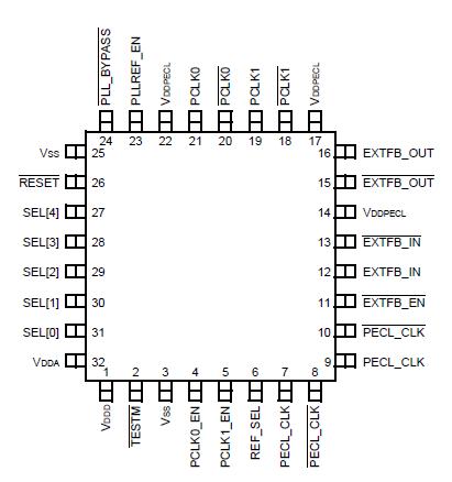
Features: Two fully selectable clock inputs. Fully integrated PLL. 336 MHz to 1 GHz output frequencies. PECL outputs. PECL reference clock.32-pin TQFP package.PinoutSpecifications Parameter Symbol Min Typical Max Unit Power Supply VDDD/VDDA 0.5 - 4.4 V V...
LCK4802: Features: Two fully selectable clock inputs. Fully integrated PLL. 336 MHz to 1 GHz output frequencies. PECL outputs. PECL reference clock.32-pin TQFP package.PinoutSpecifications Parameter ...
SeekIC Buyer Protection PLUS - newly updated for 2013!
268 Transactions
All payment methods are secure and covered by SeekIC Buyer Protection PLUS.
Parameter |
Symbol |
Min |
Typical |
Max |
Unit |
Power Supply |
VDDD/VDDA |
0.5 |
- |
4.4 |
V |
VDDHSTL |
0.5 |
- |
4.4 |
||
Input Voltage |
VIN |
0.5 |
- |
VDDD + 0.3 |
V |
Write Current |
IIN |
1 |
- |
1 |
mA |
Storage Temperature |
TS |
50 |
- |
150 |
°C |
The LCK4802 is a low-voltage, 3.3 V PECL differential clock synthesizer. The LCK4802 supports two differential PECL output pairs with frequencies from 336 MHz to 1 GHz. The clock is designed to support single and multiple processor systems that require PECL differential inputs. The LCK4802 contains a fully integrated PLL (phase-locked loop) which multiplies the PECL_CLK input frequency to match individual processor clock frequencies. The PLL can be bypassed so that the PCLK outputs are fed from the PECL_CLK or PECL_CLK input for test purposes. All outputs are powered from a 2 V external supply to reduce on-chip power consumption. All outputs are PECL. The PLL can operate in the internal feedback mode, or in the external feedback mode for board level debugging applications.