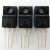
Features: • 2.8A, 250V, RDS(on) = 2.0Ω @VGS = 10 V• Low gate charge ( typical 8.1 nC)• Low Crss ( typical 7.5 pF)• Fast switching• 100% avalanche tested• Improved dv/dt capabilitySpecifications Symbol Parameter IRFW614B / IRFI614B Unit VDSS ...
IRFI614B: Features: • 2.8A, 250V, RDS(on) = 2.0Ω @VGS = 10 V• Low gate charge ( typical 8.1 nC)• Low Crss ( typical 7.5 pF)• Fast switching• 100% avalanche tested• Im...
SeekIC Buyer Protection PLUS - newly updated for 2013!
268 Transactions
All payment methods are secure and covered by SeekIC Buyer Protection PLUS.
Symbol | Parameter | IRFW614B / IRFI614B | Unit | |
VDSS |
Drain-Source Voltage |
250 | V | |
ID |
Drain Current - Continuous (TC = 25°C) |
2.8 |
A | |
1.8 |
A | |||
IDM |
Drain Current - Pulsed (Note 1) |
8.5 | A | |
VGSS | Gate-Source Voltage | ± 30 | V | |
EAS |
Single Pulsed Avalanche Energy (Note 2) | 45 | mJ | |
IAR |
Avalanche Current (Note 1) |
2.8 |
A | |
EAR |
Repetitive Avalanche Energy (Note 1) |
4.0 |
mJ | |
dv/dt |
Peak Diode Recovery dv/dt (Note 3) |
5.5 |
V/ns | |
PD |
Power Dissipation (TA = 25°C) * |
|
W | |
Power Dissipation (TC = 25°C) |
40 |
W | ||
0.32 |
W/ | |||
TJ, Tstg |
Operating and Storage Temperature Range |
-55 to +150 |
||
TL |
Maximum lead temperature for soldering purposes, |
300 |
These N-Channel enhancement mode power field effect transistors are produced using Fairchild's proprietary,planar, DMOS technology.
This advanced technology of the IRFI614B has been especially tailored to minimize on-state resistance, provide superior switching performance, and withstand high energy pulse in the avalanche and commutation mode. These devices are well suited for high efficiency switching DC/DC converters and switch mode power supplies.