Features: • Packaged in 24-pin TSSOP• Available in Pb (lead) free package• Replaces multiple crystals and oscillators• Input crystal or clock frequency of 25 MHz• Five output driver driven by external clock• Duty cycle of 45/55• Operating voltage of 3.3 V&...
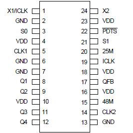
ICS680-01: Features: • Packaged in 24-pin TSSOP• Available in Pb (lead) free package• Replaces multiple crystals and oscillators• Input crystal or clock frequency of 25 MHz• Five ...
SeekIC Buyer Protection PLUS - newly updated for 2013!
268 Transactions
All payment methods are secure and covered by SeekIC Buyer Protection PLUS.
Stresses above the ratings listed below can cause permanent damage to the ICS680-01. These ratings,which are standard values for ICS commercially rated parts, are stress ratings only. Functional operation of the device at these or any other conditions above those indicated in the operational sections of the specifications is not implied. Exposure to absolute maximum rating conditions for extended periods can affect product reliability. Electrical parameters are guaranteed only over the recommended operating temperature range.
Supply Voltage, VDD .......................................7 V
All Inputs and Outputs .........-0.5 V to VDD+0.5 V
Ambient Operating Temperature ......0 to +70°C
Storage Temperature .................-65 to +150°C
Junction Temperature .............................125°C
Soldering Temperature ...........................260°C
The ICS680-01 generates four high-frequency clock outputs and a reference from a 25 MHz crystal or clock input. The device includes a low-skew, single input to four output zero delay clock buffer. It can replace multiple crystals and oscillators, saving board space and cost.
The ICS680-01 has a power-down tri-state (PDTS) pin that place the clock outputs in a high-impedance state when pulled low. The PDTS pin includes an internal pull-up resistor.