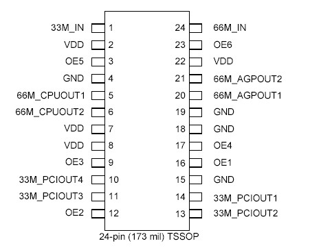
Features: • Packaged in 24-pin TSSOP• Input-output delay (±300 ps)• Two ZDB 66 MHz outputs from a 66 MHz input AGP clock• Two ZDB 66 MHz outputs, plus four 33 MHz outputs from a 33 MHz input CPU clock• Output-to-output skew is less than 250 ps• Full CMOS outputs...
ICS671-15: Features: • Packaged in 24-pin TSSOP• Input-output delay (±300 ps)• Two ZDB 66 MHz outputs from a 66 MHz input AGP clock• Two ZDB 66 MHz outputs, plus four 33 MHz outputs fro...
SeekIC Buyer Protection PLUS - newly updated for 2013!
268 Transactions
All payment methods are secure and covered by SeekIC Buyer Protection PLUS.
• Packaged in 24-pin TSSOP
• Input-output delay (±300 ps)
• Two ZDB 66 MHz outputs from a 66 MHz input AGP clock
• Two ZDB 66 MHz outputs, plus four 33 MHz outputs from a 33 MHz input CPU clock
• Output-to-output skew is less than 250 ps
• Full CMOS outputs with 18 mA output drive capability at TTL levels (at 3.3 V)
• Spread SmartTM technology works with spread spectrum clock generators
• Advanced, low-power, sub-micron CMOS process
• Operating voltage of 3.3 V
• Separate hardware output enable pins: OE1, OE2, OE3, OE4, OE5 and OE6
Item | Rating |
Supply Voltage, VDD | 7V |
All Inputs and Outputs | -0.5V to VDD+0.5V |
Ambient Operating Temperature | 0 to +70 °C |
Storage Temperature | -65 to +150°C |
Junction Temperature | 125 °C |
Soldering Temperature | 260°C |
The ICS671-15 is a low-jitter, low-skew, high-performance zero delay buffer (ZDB) for high-speed applications. The device is designed using ICS' proprietary low-jitter PLL (Phase-Locked Loop) techniques. The ICS671-15 includes a ZDB bank of four outputs running at 33 MHz, and two outputs at 66 MHz from the CPU PLL. This device also provides two 66 MHz zero delay clocks derived from the AGP PLL. In the zero delay mode, the rising edge of the input clock is aligned with the rising edges of the feedback clock. The ICS671-15 provides feedback clocks internally for the CPU PLL and the AGP PLL, and with the lowest jitter.