ICS670-01

Features: • Packaged in 16 pin SOIC• Clock inputs from 5 to 160 MHz (see page 2)• Patented PLL with the lowest phase noise• Output clocks up to 160 MHz at 3.3 V• 15 selectable on-chip multipliers• Power down mode available• Low phase noise: -124 dBc/Hz at ...

product image

ICS670-01 Picture
SeekIC No. : 004370876 Detail

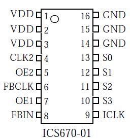
ICS670-01: Features: • Packaged in 16 pin SOIC• Clock inputs from 5 to 160 MHz (see page 2)• Patented PLL with the lowest phase noise• Output clocks up to 160 MHz at 3.3 V• 15 sel...

floor Price/Ceiling Price

Part Number:
ICS670-01
Supply Ability:
5000

Price Break

  • Qty
  • 1~5000
  • Unit Price
  • Negotiable
  • Processing time
  • 15 Days
Total Cost: $ 0.00

SeekIC Buyer Protection PLUS - newly updated for 2013!

  • Escrow Protection.
  • Guaranteed refunds.
  • Secure payments.
  • Learn more >>

Month Sales

268 Transactions

Rating

evaluate  (4.8 stars)

Upload time: 2025/3/10

Payment Methods

All payment methods are secure and covered by SeekIC Buyer Protection PLUS.

Notice: When you place an order, your payment is made to SeekIC and not to your seller. SeekIC only pays the seller after confirming you have received your order. We will also never share your payment details with your seller.
Product Details

Description


Features:

• Packaged in 16 pin SOIC
• Clock inputs from 5 to 160 MHz (see page 2)
• Patented PLL with the lowest phase noise
• Output clocks up to 160 MHz at 3.3 V
• 15 selectable on-chip multipliers
• Power down mode available
• Low phase noise: -124 dBc/Hz at 10 kHz
• Output Enable function tri-states outputs
• Low jitter 15 ps one sigma
• Full swing CMOS outputs with 25 mA drive capability at TTL levels
• Advanced, low power, sub-micron CMOS process
• Industrial temperature version available
• 3.3 V or 5 V operation


Pinout

  Connection Diagram


Specifications

Parameter
Conditions
Minimum
Typical
Maximum
Unit
Supply voltage, VDD
Referenced to GND
7
V
Inputs and Clock Outputs
Referenced to GND
-0.5
VDD+0.5
V
Ambient Operating Temperature
0
70
Ambient Operating Temperature, Iversion
Industrial temp
-40
85
Soldering Temperature
Max of 10 seconds
260
Storage temperature
-65
150


Description

The ICS670-01 is a high speed, low phase noise Zero Delay Buffer (ZDB) which integrates ICS' proprietary analog/digital Phase Locked Loop (PLL) techniques. Part of ICS' ClockBlocks™ family, the zero delay feature means that the rising edge of the input clock aligns with the rising edges of the outputs, giving the appearance of no delay through the device. There are two identical outputs on the chip. The FBCLK of the ICS670-01 should be used to connect to the FBIN. Each output has its own output enable pin.

The chip is ideal for synchronizing outputs in a large variety of systems, from personal computers to data communications to video. By allowing offchip feedback paths, the ICS670-01 can eliminate the delay through other devices. The 15 different on-chip multipliers work in a variety of applications. For other multipliers, including fractional multipliers, see the ICS527.


Customers Who Bought This Item Also Bought

Margin,quality,low-cost products with low minimum orders. Secure your online payments with SeekIC Buyer Protection.
Tapes, Adhesives
803
Integrated Circuits (ICs)
Crystals and Oscillators
Undefined Category
Cables, Wires
View more