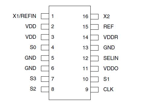
Features: • Packaged in 16-pin TSSOP
• Available in Pb-free packaging
• Clock or crystal input
• Low phase noise
• Low jitter
• Exact (0 ppm) multiplication ratios
• Power-down control
• Reference clock output available
ApplicationSeries Termination Resistor
Clock output traces should use series termination. To series terminate a 50 trace (a commonly used trace impedance), place a 33 resistor in series with the clock line, as close to the clock output pin as possible. The nominal impedance of the clock output is 20.
Decoupling Capacitors
As with any high-performance mixed-signal IC, the ICS660 must be isolated from system power supply noise to perform optimally.
Decoupling capacitors of 0.01F must be connected between each VDD and the PCB ground plane. To further guard against interfering system supply noise,
the ICS660 should use one common connection to the PCB power plane as shown in the diagram on the next page. The ferrite bead and bulk capacitor help reduce lower frequency noise in the supply that can lead to output clock phase modulation.
All power supply pins must be connected to the same voltage, except VDDR and VDDO, which may be connected to a lower voltage in order to change the
output level. If the reference output is not used, ground VDDR.
Crystal Load Capacitors
If a crystal is used, the device crystal connections should include pads for capacitors from X1 to ground and from X2 to ground. These capacitors are used to
adjust the stray capacitance of the board to match the nominally required crystal load capacitance. To reduce possible noise pickup, use very short PCB traces (and no vias) been the crystal and device.
The value of the load capacitors can be roughly determined by the formula C = 2(CL - 6) where C is the load capacitor connected to X1 and X2, and CL is the
specified value of the load capacitance for the crystal. A typical crystal CL is 18 pF, so C = 2(18 - 6) = 24 pF. Because these capacitors adjust the stray capacitance of the PCB, check the output frequency using your final layout to see if the value of C should be changed.
PCB Layout Recommendations
For optimum device performance and lowest output phase noise, the following guidelines should be observed.
1) Each 0.01F decoupling capacitor should be mounted on the component side of the board as close to the VDD pin as possible. No vias should be used
between decoupling capacitor and VDD pin. The PCB trace to VDD pin should be kept as short as possible, as should the PCB trace to the ground via. Distance of the ferrite bead and bulk decoupling from the device is less critical.
2) The external crystal should be mounted next to the device with short traces. The X1 and X2 traces shouldnot be routed next to each other with minimum spaces, instead they should be separated and away from other traces.
3) To minimize EMI, and obtain the best signal integrity, the 33 series termination resistor should be placed close to the clock output.
4) An optimum layout is one with all components on the same side of the board, minimizing vias through other signal layers (the ferrite bead and bulk decoupling capacitor can be mounted on the back). Other signal traces should be routed away from the ICS660. This includes signal traces just underneath the device, or on layers adjacent to the ground plane layer used by the device.
Pinout Specifications
Stresses above the ratings listed below can cause permanent damage to the ICS660. These ratings, which are standard values for ICS commercially rated parts, are stress ratings only. Functional operation of the device at these or any other conditions above those indicated in the operational sections of thespecifications is not implied. Exposure to absolute maximum rating conditions for extended periods can affect product reliability. Electrical parameters are guaranteed only over the recommended operating temperature range.
| Item |
Rating |
| Supply Voltage, VDD |
5.5 V |
| All Inputs and Outputs |
-0.5 V to VDD+0.5 V |
| Ambient Operating Temperature |
-40 to +85° C |
| Storage Temperature |
-65 to +150° C |
| Junction Temperature |
125° C |
| Soldering Temperature |
260° C |
DescriptionThe ICS660 provides clock generation and conversion for clock rates commonly needed in digital video equipment, including rates for MPEG, NTSC, PAL, and
HDTV. The ICS660 uses the latest PLL technology to provide excellent phase noise and long term jitter performance for superior synchronization and S/N
ratio.
For audio sampling clocks generated from 27 MHz, usethe ICS661.
Please contact ICS of the ICS660 if you have a requirement for an input and output frequency not included here - we can rapidly modify this product to meet special requirements.

 ICS660 Data Sheet


