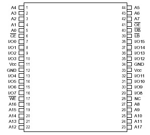
Features: • High-speed access times: 55, 70, 100 ns• CMOS low power operation ICC1=10mA (typical)* operating ISB2=1µA (typical)* CMOS standby• Typical values are measured at VCC=1.8V, TA=25°C• TTL compatible interface levels• Single 1.65V-2.2V Vcc power supply...
IC62VV25616LL: Features: • High-speed access times: 55, 70, 100 ns• CMOS low power operation ICC1=10mA (typical)* operating ISB2=1µA (typical)* CMOS standby• Typical values are measured at ...
SeekIC Buyer Protection PLUS - newly updated for 2013!
268 Transactions
All payment methods are secure and covered by SeekIC Buyer Protection PLUS.
Features: • High-speed access time: 35, 45, 55, 70 ns• Low active power: 450 mW (typic...
Features: • Access times of 55, 70, 100 ns• CMOS Low power operation: ICC=15mA (typica...
SYMBOL |
PARAMETER |
VALUE |
UNIT |
VTERM |
Terminal Voltage with Respect to GND |
0.5 to Vcc + 0.4 |
V |
TBIAS |
Temperature Under Bias |
40 to +85 |
°C |
VCC |
Vcc related to GND |
0.3 to +4.0 |
V |
TSTG |
Storage Temperature |
65 to +150 |
°C |
PT |
Power Dissipation |
1.0 |
W |
The IC62VV25616LL are low-power, 4.194,304 bit static RAMs organized as 262,144 words by 16 bits. They are fabricated using ICSI's high-performance CMOS technology. This highly reliable process coupled with innovative circuit design techniques, yields high-performance and low power consumption devices.
When CE of the IC62VV25616LL is HIGH (deselected) or both LB and UB are HIGH, the device assumes a standby mode at which the power dissipation can be reduced by using CMOS input levels. Easy memory expansion is provided by using Chip Enable Output and Enable inputs, CE and OE. The active LOW Write Enable (WE) controls both writing and reading of the memory. A data byte allows Upper Byte (UB) and Lower Byte (LB) access.
The IC62VV25616LL are packaged in the JEDEC standare 44-pin TSOP-2 and 48-pin 6*8mm TF-BGA.