IC42S16102

Features: • Driver Strength for High capacitive bus loading• Clock frequency: 200, 166, 143 MHz• Fully synchronous; all signals referenced to apositive clock edge• Two banks can be operated simultaneously andindependently• Dual internal bank controlled by A11 (bank se...

product image

IC42S16102 Picture
SeekIC No. : 004370376 Detail

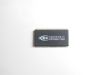
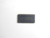
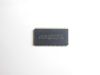
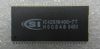
IC42S16102: Features: • Driver Strength for High capacitive bus loading• Clock frequency: 200, 166, 143 MHz• Fully synchronous; all signals referenced to apositive clock edge• Two banks ...

floor Price/Ceiling Price

Part Number:
IC42S16102
Supply Ability:
5000

Price Break

  • Qty
  • 1~5000
  • Unit Price
  • Negotiable
  • Processing time
  • 15 Days
Total Cost: $ 0.00

SeekIC Buyer Protection PLUS - newly updated for 2013!

  • Escrow Protection.
  • Guaranteed refunds.
  • Secure payments.
  • Learn more >>

Month Sales

268 Transactions

Rating

evaluate  (4.8 stars)

Upload time: 2024/5/27

Payment Methods

All payment methods are secure and covered by SeekIC Buyer Protection PLUS.

Notice: When you place an order, your payment is made to SeekIC and not to your seller. SeekIC only pays the seller after confirming you have received your order. We will also never share your payment details with your seller.
Product Details

Description


Features:

• Driver Strength for High capacitive bus loading
• Clock frequency: 200, 166, 143 MHz
• Fully synchronous; all signals referenced to a
positive clock edge
• Two banks can be operated simultaneously and
independently
• Dual internal bank controlled by A11 (bank select)
• Single 3.3V power supply
• LVTTL interface
• Programmable burst length
(1, 2, 4, 8, full page)
• Programmable burst sequence:
Sequential/Interleave
• Auto refresh, self refresh
• 4096 refresh cycles every 64 ms
• Random column address every clock cycle
• Programmable CAS latency (2, 3 clocks)
• Burst read/write and burst read/single write
operations capability
• Burst termination by burst stop and precharge
command
• Byte controlled by LDQM and UDQM
• Package 400mil 50-pin TSOP-2 and 60ball(16M)
VF-BGA
• Pb(lead)-free package is available


Pinout

  Connection Diagram


Specifications

Symbol Parameters Rating Unit
VDD MAX Maximum Supply Voltage 1.0 to +4.6 V
VDDQ MAX Maximum Supply Voltage for Output Buffer 1.0 to +4.6 V
VIN Input Voltage 1.0 to +4.6 V
VOUT Output Voltage 1.0 to +4.6 V
PD MAX Allowable Power Dissipation 1 W
ICS Output Shorted Current 50 mA
TOPR Operating Temperature 0 to +70
TSTG Storage Temperature 55 to +150


Description

ICSI's 16Mb Synchronous DRAM IC42S16102 is organized as a 524,288-word x 16-bit x 2-bank for improved performance. The synchronous DRAMs achieve high-speed data transfer using pipeline architecture. All inputs and outputs signals refer to the rising edge of the clock input.


Customers Who Bought This Item Also Bought

Margin,quality,low-cost products with low minimum orders. Secure your online payments with SeekIC Buyer Protection.
Tapes, Adhesives
803
Potentiometers, Variable Resistors
Power Supplies - Board Mount
LED Products
View more