HYMP532U646-E3

Features: • JEDEC standard Double Data Rate2 Synchrnous DRAMs (DDR2 SDRAMs) with 1.8V +/- 0.1V Power Supply• All inputs and outputs are compatible with SSTL_1.8 interface• 4 Bank architecture• Posted CAS• Programmable CAS Latency 3 , 4 , 5• OCD (Off-Chip Driver ...

product image

HYMP532U646-E3 Picture
SeekIC No. : 004369340 Detail

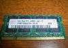
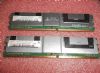
HYMP532U646-E3: Features: • JEDEC standard Double Data Rate2 Synchrnous DRAMs (DDR2 SDRAMs) with 1.8V +/- 0.1V Power Supply• All inputs and outputs are compatible with SSTL_1.8 interface• 4 Bank a...

floor Price/Ceiling Price

Part Number:
HYMP532U646-E3
Supply Ability:
5000

Price Break

  • Qty
  • 1~5000
  • Unit Price
  • Negotiable
  • Processing time
  • 15 Days
Total Cost: $ 0.00

SeekIC Buyer Protection PLUS - newly updated for 2013!

  • Escrow Protection.
  • Guaranteed refunds.
  • Secure payments.
  • Learn more >>

Month Sales

268 Transactions

Rating

evaluate  (4.8 stars)

Upload time: 2024/5/28

Payment Methods

All payment methods are secure and covered by SeekIC Buyer Protection PLUS.

Notice: When you place an order, your payment is made to SeekIC and not to your seller. SeekIC only pays the seller after confirming you have received your order. We will also never share your payment details with your seller.
Product Details

Description


Features:

• JEDEC standard Double Data Rate2 Synchrnous DRAMs (DDR2 SDRAMs) with 1.8V +/- 0.1V Power Supply
• All inputs and outputs are compatible with SSTL_1.8 interface
• 4 Bank architecture
• Posted CAS
• Programmable CAS Latency 3 , 4 , 5
• OCD (Off-Chip Driver Impedance Adjustment)
• ODT (On-Die Termination)
• Fully differential clock operations (CK & CK)
• Programmable Burst Length 4 / 8 with both sequential and interleave mode
• Auto refresh and self refresh supported
• 8192 refresh cycles / 64ms
• Serial presence detect with EEPROM
• DDR2 SDRAM Package: 60ball FBGA(64Mx8), 84ball FBGA(32Mx16)
• 133.35 x 30.00 mm form factor
• Lead-free Products are RoHS compliant


Specifications

Parameter
Symbol
Value
Unit
Note
Voltage on VDD pin relative to Vss
VDD
- 1.0 V ~ 2.3 V
V
1
Voltage on VDDL pin relative to Vss
VDDL
-0.5V ~ 2.3 V
V
1
Voltage on VDDQ pin relative to Vss
VDDQ
- 0.5 V ~ 2.3 V
V
1
Voltage on any pin relative to Vss
VIN,VOUT
- 0.5 V ~ 2.3 V
V
1
Storage Temperature
TSTG
-50 ~ +100
1
Storage Humidity(without condensation)
HSTG
5 to 95
%
1
Notes :
1. Stress greater than those listed may cause permanent damage to the device. This is a stress rating only, and device functional operation at or above the conditions indicated is not implied.
Expousure to absolute maximum rating conditions for extended periods may affect reliablility.


Customers Who Bought This Item Also Bought

Margin,quality,low-cost products with low minimum orders. Secure your online payments with SeekIC Buyer Protection.
Semiconductor Modules
Isolators
Soldering, Desoldering, Rework Products
Resistors
Connectors, Interconnects
Test Equipment
View more