Features: 32-bit ARM7TDMI RISC static CMOS CPU core (Running up to 60 MHz)
8Kbytes combined instruction/data cache
Memory management unit
Supports Little-endian operating system
8Kbytes SRAM for internal buffer memory
2Kbytes Boot ROM
On-chip peripherals with individual power-down:
·Memory controller for ROM(x8,16), Flash(x8,16), SRAM(x8,16), SDRAM(x16)
·5-State Power management unit (Sofrware selectable Clock Frequency)
·Interrupt Controller
·LCD Controller for color and mono STN
·USB 1.1(slave)
·Two Smart Card Interface (UART 0,1)
·Two UART (UART 2,3)
·One SIR support UART (UART4)
·One Modem support UART (UART5)
·Four 16-bit Timer Channels (with Output Port)
·Two 16-bit PWM Channels (with Output Port)
·Programmable WatchDog Timer with On-chip Oscillator
·Real-time clock (32.768kHz oscillator) with separated Vcc
·Matrix Keyboard control interface (6x6)
·97 Programmable GPIO
·One 2-Wire Serial Bus Interface
·2-Channel Master/Slave SSI (SPI)
·SMC Card Interface
·On-chip 3-Channel 10-bit ADC
JTAG debug interface and boundary scan
0.35um CMOS Process
3.3V supply voltage
208-pin LQFP / CABGA package
Low power consumptionPinout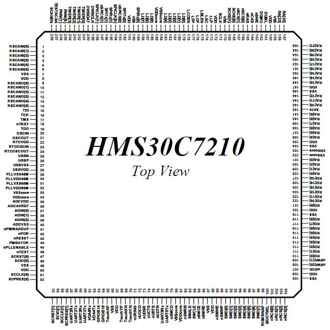 Specifications
Symbol |
Parameter |
Typical |
Units |
VDD Condition |
PRUN |
RUN Mode Power |
391 |
mW |
@ 3.3V |
PSLOW |
SLOW Mode Power |
355 |
mW |
@ 3.3V |
PIDLE |
IDLE Mode Power |
276 |
mW |
@ 3.3V |
PPD |
Deep-Sleep Mode Power |
3.3 |
uW |
@ 3.3V |
PRTC |
RTC Power |
36 |
uW |
@ 3.3V |
DescriptionThe SSI HMS30C7210 is reset by nSSPRST and it is generated by the global reset signal BnRES or the test reset signal in SSI test mode. An external reset controller must use BnRES to reset the whole SSI including test logic. The test reset signal resets SSI registers except for test mode registers.
Following the reset, the SSI HMS30C7210 is disabled and should be configured in this state. Control register SSPCR0 need to be programmed to decide several operation parameters.
GSEL bit determines whether nSFRMIN signal from the GPIO is used in slave mode.
If GSEL bit is cleared, the SSI HMS30C7210 regards nSFRMIN signal as zero and transfers are synchronized only with SCLKIN clock signal. If GSEL bit is set, nSFRMIN signal from a GPIO pin is used to indicate valid SCLKIN period and transfers are synchronized with SCLKIN when nSFRMIN is zero. In master mode, GSEL bit has no effects and nSFRMOUT signal to a GPIO pin is always valid. SDIR bit is used to determine the direction of nSFRMIN/OUT and SCLKIN/OUT pins in the GPIO. When SDIR bit is set, the direction is output and nSFRMOUT and SCLKOUT signals go out through GPIO pins. MS bit configures the SSI HMS30C7210 as a master or slave and SPH and SPO bits determine clock phase and polarity respectively.
When master, the bit rate requires the programming of the clock scale register SSPCSR. The SSPCR1 has SSI the HMS30C7210 enable (SSE) and interrupts enable bits. When disabled in master mode, SCLKOUT is forced to LOW (SPO=0) or HIGH (SPO=1), nSFRMOUT to HIGH, and SSPTXD to LOW. When disabled in slave mode, SCLKIN, nSFRMIN and SSPRXD has no meanings and SSPTXD is set to LOW. Once enabled, transmission and reception of data begins on transmit (SSPTXD) and receive (SSPRXD) pins.
NOTE about the HMS30C7210: When nSFRMIN/OUT signal from/to a GPIO pin is not connected, SDIR and SPO bits in a master should be configured before a slave is enable. Otherwise, the transition of SCLKOUT generated by setting CDIR and/or SPO in the master may cause the slave into malfunctioning. In this case, the recommended sequence of register setup is following. SSPCR0 register in a master should be configured first. Then SSPCR0 in a slave is set and a slave SSI is enabled. The master is enabled last.
About the HMS30C7210, once the bottom entry of the transmit FIFO in a master contains data, nSFRMOUT is active to LOW to indicate valid data frame and the MSB of the 8-bit data frame is shifted out onto the SSPTXD pin. Then, SCLKOUT pin starts running and the serial data bit through SSPRXD is captured in the receive FIFO. After the LSB of the current data frame is shifted out, if there is no more valid entry in the transmit FIFO, SCLKOUT stops toggling and nSFRMOUT is inactive to indicate the completion of the transfer. Otherwise, any valid entries in the transmit FIFO enables another data frame transfer to be continued without delay. Figure 9-7. shows the frame format for a single frame and Figure 9-8. shows the timing diagram when back to back frames are transmitted.
About the HMS30C7210, If the receive FIFO is already full and the transmit FIFO is not empty in master mode, a transfer will start but this transfer will cause receive overrun interrupt condition. In this case, a transmit data frame is read from the transmit FIFO and transferred, and a received data frame is overwritten in the receive serial shift buffer normally. But, data in the receive serial buffer will not be stored in the receive FIFO, if the receive FIFO is still full until this transfer finishes. If RORIE bit is set for the receive overrun condition, SSPRORINTR will signal and further data frame will not start until RORIS bit is cleared. In case of slave mode, the operation is the same except that a data framestarts with SCLKIN from external device.
About the HMS30C7210, If the transmit FIFO is already empty and another data frame is request in slave mode, a transmit FIFO underrun condition occurs. The receive FIFO operates normally but transmit FIFO transfers the same data frame as in the previous transfer. This condition cannot occur in master mode. In this version of SSI, there is not an assigned interrupt for this case.
About the HMS30C7210, If CPU writes data to the transmit FIFO that is already full, the valid entries (from the oldest entry that was written) in the FIFO can be overwritten. To detect this erroneous state, TXENT bits can be read. If TXENT[3:0] is in the range of from 0x9 to 0xf, the number of lost entries is TXENT - 0x8.

 HMS30C7210 Data Sheet


