FMS7951

Features: • Low Voltage CMOS or PECL reference input• Up to 175 MHz of output frequency• Nine configurable outputs• Output enable pin• 250 pS of output to output skew• 300 pS of Cycle to Cycle Jitter• VDDRange of 3.3V ±0.2V • Commercial temperature r...

product image

FMS7951 Picture
SeekIC No. : 004342878 Detail

FMS7951: Features: • Low Voltage CMOS or PECL reference input• Up to 175 MHz of output frequency• Nine configurable outputs• Output enable pin• 250 pS of output to output skew&#...

floor Price/Ceiling Price

Part Number:
FMS7951
Supply Ability:
5000

Price Break

  • Qty
  • 1~5000
  • Unit Price
  • Negotiable
  • Processing time
  • 15 Days
Total Cost: $ 0.00

SeekIC Buyer Protection PLUS - newly updated for 2013!

  • Escrow Protection.
  • Guaranteed refunds.
  • Secure payments.
  • Learn more >>

Month Sales

268 Transactions

Rating

evaluate  (4.8 stars)

Upload time: 2024/12/21

Payment Methods

All payment methods are secure and covered by SeekIC Buyer Protection PLUS.

Notice: When you place an order, your payment is made to SeekIC and not to your seller. SeekIC only pays the seller after confirming you have received your order. We will also never share your payment details with your seller.
Product Details

Description


Features:

• Low Voltage CMOS or PECL reference input
• Up to 175 MHz of output frequency
• Nine configurable outputs
• Output enable pin
• 250 pS of output to output skew
• 300 pS of Cycle to Cycle Jitter
• VDDRange of 3.3V ±0.2V
• Commercial temperature range
• Available in 32 pin TQFP


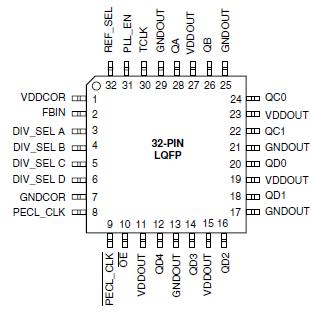
Pinout

  Connection Diagram


Specifications

Symbol Parameter Ratings Units
VDD, VIN Voltage on any pin with respect to ground 0.5 to 7.0 V
TSTG Storage Temperature 65 to 150
TB Ambient Temperature 55 to 125
TA Operating Temperature 0 to 70

Stresses greater than those listed in the table may cause permanent damage to the device. These represent a stress rating only.

Operation of the device at these or any other conditions above those specified in the operating sections of this specification is not implied. Maximum conditions for extended periods may effect reliability.


Description

FMS7951 is a high speed, zero delay, low skew clock driver. It uses phase locked loop technology to generate frequencies up to 175 MHz.

FMS7951 has four banks of configurable outputs. By externally connecting one of the outputs to FBIN, the internal PLL will lock in both phase and frequency to the incoming clock. Any changes to the input clock will be tracked by the outputs.

Depending on the selected output for feedback connection, the output frequencies of FMS7951 will be as 1X, 2X or 4X of the input.

REF_SEL allows selection between PECL input or TCLK a CMOS clock driven input. Connecting PLL_EN LOW and REF_SEL HIGH will by pass the Phase locked loop. In this mode, FMS7951 will be in clock buffer mode where any clock applied to TCLK will be divided down to the four output banks. This is ideal for system diagnostic test. When PLL_EN is HIGH, the PLL is enabled, and any clock applied to TCLK will be locked in both phase and frequency to FBIN. PECL_CLK is activated when REF_SEL is high.

FMS7951 operates at 3.3 Volts and is available in 32 pin LQFP.


Customers Who Bought This Item Also Bought

Margin,quality,low-cost products with low minimum orders. Secure your online payments with SeekIC Buyer Protection.
Sensors, Transducers
Audio Products
Potentiometers, Variable Resistors
View more