Features: 9-bit Inverting BTL transceiver meets IEEE 1194.1standard on Backplane Transceiver Logic (BTL)
Supports live insertion
Glitch free power-up/down protection
Typically less than 5 pF bus-port capacitance
Low bus-port voltage swing (typically 1V) at 80 mA
Open collector bus-port output allows Wired-OR
Controlled rise and fall time to reduce noise coupling
TTL compatible driver and control inputs
Built in bandgap reference with separate QV CC andQGND pins for precise receiver thresholds
Exceeds 2 kV ESD (Human Body Model)
Individual bus-port ground pins minimize ground bounce
Tight skew (1 ns typical)Pinout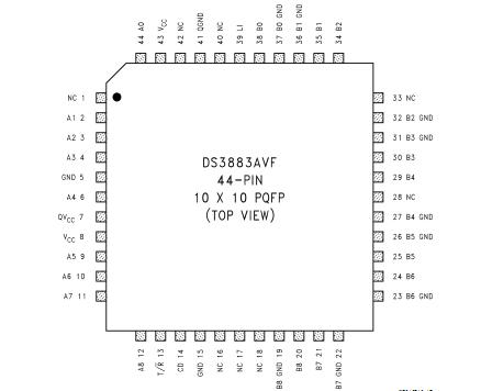 SpecificationsSupply Voltage.............................................. 6.5V
Control Input Voltage ...................................6.5V
Driver Input and Receiver Output .... ............5.5V
Receiver Input Current........................... ±15 mA
Bus Termination Voltage.............................. 2.4V
Power Dissipation at ....................................25
PQFP (VF44B) ..............................................1.3W
Derate PQFP Package (VF44B) ..........11.1 mW/˚C
Storage Temperature Range .....−65˚C to +150˚C
Lead Temperature
(Soldering, 4 seconds) ...............................260˚CDescriptionThe DS3883A receiver is a high speed comparator that utilizes a band-gap reference for precision threshold control allowing maxi-mum noise immunity to the BTL 1V signaling level. SeparateQVCC and QGND pins are provided to minimize the effectsof high current switching noise. The output is TRI-STATE®and fully TTL compatible.
The DS3883A supports live insertion as defined in 896.2through the LI (Live Insertion) pin. To implement live inser-tion the LI pin should be connected to the live insertionpower connector. If this function is not supported the LI pinmust be tied to the VCC pin. The DS3883A also providesglitch free power up/down protection during power sequenc-ing.
The DS3883A has two types of power connections in addi-tion to the LI pin. They are the Logic VCC (VCC) and the QuietVCC (QVCC). There are two logic VCC pins on the DS3883that provide the supply voltage for the logic and control cir-cuitry. Multiple power pins reduce the effects of package in-ductance and thereby minimize switching noise. As thesepins are common to the V CC bus internal to the device, avoltage delta should never exist between these pins and thevoltage difference between VCC and QV CC should never ex-ceed ±0.5V because of ESD circuitry.
Additionally, the ESD circuitry between the VCC pins and allother pins except for BTL I/O's and LI pins requires that anyvoltage on these pins should not exceed the voltage on VCC+ 0.5V.
There are three different types of ground pins on theDS3883A. They are the logic ground (GND), BTL grounds(B0GNDB8GND) and the Bandgap reference ground(QGND). All of these ground reference pins are isolatedwithin the chip to minimize the effects of high current switch-ing transients. For optimum performance the QGND shouldbe returned to the connector through a quiet channel thatdoes not carry transient switching current. The GND andB0GNDB8GND should be connected to the nearest back-plane ground pin with the shortest possible path.
Since many different grounding schemes could be imple-mented and ESD circuitry exists on the DS3883, it is impor-ant to note that any voltage difference between ground pins,QGND, GND or B0GNDB8GND should not exceed ±0.5Vncluding power-up/down sequencing.
When CD (Chip Disable) is high, An and Bn are in a high im-pedance state. To transmit data (An to Bn) the T/R signal ishigh. To receive data (Bn to An) the T/R signal is low.

 DS3883A Data Sheet