Am28F512

PinoutDescriptionThe Am28F512 is a 512 K bit Flash memory organized as 64 Kbytes of 8 bits each. AMD's Flash memories offer the most cost-effective and reliable read/ write non-volatile random access memory. The Am28F512 is packaged in 32-pin PDIP, PLCC, and TSOP versions. It is designed to be rep...

product image

Am28F512 Picture
SeekIC No. : 004282183 Detail

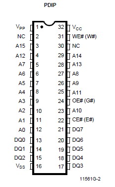
Am28F512: PinoutDescriptionThe Am28F512 is a 512 K bit Flash memory organized as 64 Kbytes of 8 bits each. AMD's Flash memories offer the most cost-effective and reliable read/ write non-volatile random acces...

floor Price/Ceiling Price

Part Number:
Am28F512
Supply Ability:
5000

Price Break

  • Qty
  • 1~5000
  • Unit Price
  • Negotiable
  • Processing time
  • 15 Days
Total Cost: $ 0.00

SeekIC Buyer Protection PLUS - newly updated for 2013!

  • Escrow Protection.
  • Guaranteed refunds.
  • Secure payments.
  • Learn more >>

Month Sales

268 Transactions

Rating

evaluate  (4.8 stars)

Upload time: 2024/7/15

Payment Methods

All payment methods are secure and covered by SeekIC Buyer Protection PLUS.

Notice: When you place an order, your payment is made to SeekIC and not to your seller. SeekIC only pays the seller after confirming you have received your order. We will also never share your payment details with your seller.
Product Details

Description


Pinout

  Connection Diagram


Description

The Am28F512 is a 512 K bit Flash memory organized as 64 Kbytes of 8 bits each. AMD's Flash memories offer the most cost-effective and reliable read/ write non-volatile random access memory. The Am28F512 is packaged in 32-pin PDIP, PLCC, and TSOP versions. It is designed to be reprogrammed and erased in-system or in standard EPROM programmers. The Am28F512 is erased when shipped from the factory.

The standard Am28F512 offers access times as fast as 70 ns, allowing operation of high-speed microprocessors without wait states. To eliminate bus contention, the Am28F512 has separate chip enable (CE#) and output enable (OE#) controls.

AMD's Flash memories augment EPROM functionality with in-circuit electrical erasure and programming. The Am28F512 uses a command register to manage this functionality, while maintaining a standard JEDEC Flash Standard 32-pin pinout. The command register allows for 100% TTL level control inputs and fixed power supply levels during erase and programming.

AMD's Flash technology reliably stores memory contents even after 10,000 erase and program cycles. The AMD cell is designed to optimize the erase and programming mechanisms. In addition, the combination of advanced tunnel oxide processing and low internal electric fields for erase and programming operations produces reliable cycling. The Am28F512 uses a 12.0V±5% VPP high voltage input to perform the Flasherase and Flashrite algorithms.

The highest degree of latch-up protection is achieved with AMD's proprietary non-epi process. Latch-up protection is provided for stresses up to 100 mA on address and data pins from -1 V to VCC +1 V.

The Am28F512 is byte programmable using 10 ms programming pulses in accordance with AMD's Flashrite programming algorithm. The typical room temperatureprogramming time of the Am28F512 is one second. 

The entire chip is bulk erased using 10 ms erase pulses according to AMD's Flasherase algorithm. Typical erasure at room temperature is accomplished in less than one second. The windowed package and the 15-20 minutes required for EPROM erasure using ultra-violet light are eliminated. Commands are written to the command register using standard microprocessor write timings. Register contents serve as inputs to an internal state-machine which controls the erase and programming circuitry. During


Customers Who Bought This Item Also Bought

Margin,quality,low-cost products with low minimum orders. Secure your online payments with SeekIC Buyer Protection.
Transformers
Soldering, Desoldering, Rework Products
Static Control, ESD, Clean Room Products
Cables, Wires - Management
LED Products
View more