Features: • AS7C4098 (5V version)
• AS7C34098 (3.3V version)
• Industrial and commercial temperature
• Organization: 262,144 words * 16 bits
• Center power and ground pins
• High speed
- 10/12/15/20 ns address access time
- 5/6/7/8 ns output enable access time
• Low power consumption: ACTIVE
- 1375 mW (AS7C4098)/max @ 12 ns
- 576 mW (AS7C34098)/max @ 10 ns
• Low power consumption: STANDBY
- 110 mW (AS7C4098)/max CMOS
- 72 mW (AS7C34098)/max CMOS
• Individual byte read/write controls
• Easy memory expansion with CE, OE inputs
• TTL- and CMOS-compatible, three-state I/O
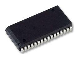
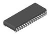
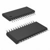
• 44-pin JEDEC standard packages
- 400-mil SOJ
- TSOP 2
• ESD protection 2000 volts
• Latch-up current 100 mAPinout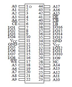 Specifications
|
Parameter |
Device |
Symbol |
Min |
Max |
Unit |
| Voltage on VCC relative to GND |
AS7C4098 |
Vt1 |
-0.5 |
+7.0 |
V |
| AS7C34098 |
Vt1 |
-0.5 |
+5.0 |
| Voltage on any pin relative to GND |
|
Vt2 |
-0.5 |
VCC + 0.5 |
V |
| Power Dissipation |
|
Pd |
- |
1.5 |
W |
| DC current into outputs (low) |
|
IOUT |
- |
±20 |
mA |
| Storage temperature (plastic) |
|
Tstg |
65 |
+150 |
°C |
| Ambient temperature with VCC applied |
|
Tbias |
55 |
+125 |
°C |
Note: Stresses greater than those listed under Absolute Maximum Ratings may cause permanent damage to the device. This is a stress rating only and functional operation of the device at these or any other conditions outside those indicated in the operational sections of this specification is not implied.Exposure to absolute maximum rating conditions for extended periods may affect reliability.
DescriptionThe AS7C4098 and AS7C34098 are high-performance CMOS 4,194,304-bit Static Random Access Memory (SRAM) devices organized as 262,144 words * 16 bits. They are designed for memory applications where fast data access, low power, and simple interfacing are desired.
Equal address of AS7C4098 access and cycle times (tAA, tRC, tWC) of 10/12/15/20 ns with output enable access times (tOE) of 5/6/7/8 ns are ideal for high-performance applications. The chip enable input CE permits easy memory expansion with multiple-bank memory systems.
When CE is HighAS7C4098 enters standby mode. The standard AS7C4098/AS7C34098 is guaranteed not to exceed 110/72mW power consumption in CMOS standby mode. A write cycle is accomplished by asserting write enable (WE) and chip enable (CE). Data on the input pins I/O1I/O16 is written on the rising edge of WE (write cycle 1) or CE (write cycle 2). To avoid bus contention, external devices of AS7C4098 should drive I/O pins only after outputs have been disabled with output enable (OE) or write enable (WE).
A read cycle of AS7C4098 is accomplished by asserting output enable (OE) and chip enable (CE), with write enable (WE) High. The chip drives I/O pins with the data word referenced by the input address. When either chip enable or output enable is inactive, or write enable is active, output drivers stay in high-impedance mode.
AS7C4098 provide multiple center power and ground pins, and separate byte enable controls, allowing individual bytes to be written and read. LB controls the lower bits, I/O1I/O8, and UB controls the higher bits, I/O9I/O16.
All chip inputs and outputs of AS7C4098 are TTL- and CMOS-compatible, and operation is from either a single 5V (AS7C4098) or 3.3V (AS7C34098) supply. Both devices are available in the JEDEC standard 400-mL, 44-pin SOJ and TSOP 2 packages.

 AS7C4098 Data Sheet