Features: •Industrial and commercial versions
•Organization: 65,536 words * 16 bits
•Center power and ground pins for low noise
•High speed
-10/12/15/20 ns address access time
-5, 6, 7, 8 ns output enable access time
•Low power consumption: ACTIVE
-288 mW / max @ 10 ns
•Low power consumption: STANDBY
-18 mW / max CMOS I/O
•6 T 0.18 u CMOS technology
•Easy memory expansion with CE</a>, OE</a> inputs
•TTL-compatible, three-state I/O
•JEDEC standard packaging
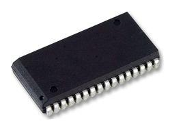
-44-pin 400 mil SOJ
-44-pin TSOP 2-400
•ESD protection 2000 volts
•Latch-up current 200 mAPinout Specifications
| Parameter |
Symbol |
Min |
Max |
Unit |
| Voltage on VCC relative to GND |
Vt1 |
0.50 |
+5.0 |
V |
| Voltage on any pin relative to GND |
Vt2 |
0.50 |
VCC +0.50 |
V |
| Power dissipation |
PD |
|
1.0 |
W |
| Storage temperature (plastic) |
Tstg |
65 |
+150 |
°C |
| Ambient temperature with VCC applied |
Tbias |
55 |
+125 |
°C |
| DC current into outputs (low) |
IOUT |
|
20 |
mA |
DescriptionThe AS7C31026B is a high-performance CMOS 1,048,576-bit Static Random Access Memory (SRAM) device organized as 65,536 words× 16 bits. It is designed for memory applications where fast data access, low power, and simple interfacing are desired.
Equal address access and cycle times (tAA, tRC, tWC) of 10/12/15/20 ns with output of AS7C31026B enable access times (tOE) of 5, 6, 7, 8 ns are ideal for high-performance applications.
When CE</a> is high, AS7C31026B enters standby mode.A write cycle is accomplished by asserting write enable (WE</a>) and chip enable (CE</a>). Data on the input pins I/O0 through I/O15 is written on the rising edge of WE</a> (write cycle 1) or CE</a> (write cycle 2). To avoid bus contention,external devices of AS7C31026B should drive I/O pins only after outputs have been disabled with output enable (OE</a>) or write enable (WE</a>).
A read cycle of AS7C31026B is accomplished by asserting output enable (OE</a>) and chip enable (CE</a>) with write enable (WE</a>) high. The AS7C31026B drive I/O pins with the data word referenced by the input address. When either chip enable or output enable is inactive or write enable is active, output drivers stay in high-impedance mode.
AS7C31026B provides multiple center power and ground pins, and separate byte enable controls, allowing individual bytes to be written and read. LB</a>
controls the lower bits, I/O0 through I/O7, and UB</a> controls the higher bits, I/O8 through I/O15.
All chip inputs of AS7C31026B and outputs are TTL-compatible, and operation is from a single 3.3 V supply. The device is packaged in common industry standard packages.

 AS7C31026B Data Sheet


