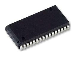
Features: •Organization: 32,768 words * 8 bits•High speed10/12/15/20/25/35 ns address access time3/3/4/5/6/8 ns output enable access time•Low power consumptionActive:660 mW max (10 ns cycle)Standby:11 mW max, CMOS I/O 2.75 mW max, CMOS I/O, L versionVery low DC component in activ...
AS7C256L: Features: •Organization: 32,768 words * 8 bits•High speed10/12/15/20/25/35 ns address access time3/3/4/5/6/8 ns output enable access time•Low power consumptionActive:660 mW max (10...
SeekIC Buyer Protection PLUS - newly updated for 2013!
268 Transactions
All payment methods are secure and covered by SeekIC Buyer Protection PLUS.
Features: `AS7C1024A (5V version)` AS7C31024A (3.3V version)` Industrial and commercial temperatur...
PARAMETER |
SYMBOL |
MIN |
MAX |
UNIT |
Voltage on Any Pin Relative to GND |
Vt |
0.5 |
+7.0 |
V |
Power Dissipation |
PD |
1.0 |
W | |
Storage Temperature (Plastic) |
Tstg |
55 |
+150 |
oC |
Temperature Under Bias |
Tbias |
10 |
+85 |
oC |
DC Output Current |
Iout |
20 |
mA |
The AS7C256 is a high performance CMOS 262,144-bit Static Random Access Memory (SRAM) organized as 32,768 words × 8 bits. It is designed for memory applica- tions where fast data access, low power, and simple interfac- ing are desired.
Equal address access and cycle times (tAA, tRC, tWC) of10/12/15/20/25/35 ns with output enable access times (tOE)of 3/3/4/5/6/8 ns are ideal for high performance applica-tions. A chip enable CE input permits easy memory expansion with multiple-bank memory organizations.
When CE is HIGH the device enters standby mode. The standard AS7C256 is guaranteed not to exceed 11 mW power consumption in standby mode; the L version is guar-anteed not to exceed 2.75 mW, and typically requires only 500 µW. The L version also offers 2.0V data retention, with maximum power consumption in this mode of 300 µW.
A write cycle is accomplished by asserting chip enable (CE)and write enable (WE) LOW. Data on the input pins I/O0-I/O7 is written on the ri sing edge of WE (write cycle 1)or CE (write cycle 2). To avoid bus contention, external devices should drive I/O pins only after outputs have been disabled with output enable (OE ) or write enable (WE).
A read cycle is accomplished by asserting chip enable (CE)and output enable (OE) LOW, with write enable (WE) HIGH. The chip drives I/O pins with the data word refer-enced by the input address. When chip enable or output enable is HIGH, or write enable is LOW, output drivers stay in high-impedance mode.
All chip inputs and outputs are TTL-compatible, and opera- tion is from a single 5V supply. The AS7C256 is packaged in all high volume industry standard packages.