74F533

Features: • 8-bit positive edge-triggered register 74F534• 3-State inverting output buffers• Common 3-State Output register• Independent register and 3-State buffer operationPinoutSpecifications SYMBOL PARAMETER RATING UNIT VCC Supply voltage 0.5 to ...

product image

74F533 Picture
SeekIC No. : 004249790 Detail

74F533: Features: • 8-bit positive edge-triggered register 74F534• 3-State inverting output buffers• Common 3-State Output register• Independent register and 3-State buffer operatio...

floor Price/Ceiling Price

Part Number:
74F533
Supply Ability:
5000

Price Break

  • Qty
  • 1~5000
  • Unit Price
  • Negotiable
  • Processing time
  • 15 Days
Total Cost: $ 0.00

SeekIC Buyer Protection PLUS - newly updated for 2013!

  • Escrow Protection.
  • Guaranteed refunds.
  • Secure payments.
  • Learn more >>

Month Sales

268 Transactions

Rating

evaluate  (4.8 stars)

Upload time: 2024/11/24

Payment Methods

All payment methods are secure and covered by SeekIC Buyer Protection PLUS.

Notice: When you place an order, your payment is made to SeekIC and not to your seller. SeekIC only pays the seller after confirming you have received your order. We will also never share your payment details with your seller.
Product Details

Description


Features:

• 8-bit positive edge-triggered register 74F534
• 3-State inverting output buffers
• Common 3-State Output register
• Independent register and 3-State buffer operation


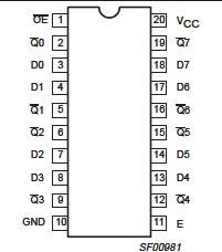
Pinout

  Connection Diagram


Specifications

SYMBOL
PARAMETER
RATING
UNIT
VCC Supply voltage
0.5 to +7.0
V
VIN Input voltage
0.5 to +7.0
V
IIN Input current
30 to +5
mA
VOUT Voltage applied to output in high output state
0.5 to VCC
V
IOUT Current applied to output in low output state
48
mA
Tamb Operating free air temperature range
0 to +70
°C
Tstg Storage temperature range
65 to +125
°C


Description

The 74F533 is an octal transparent latch coupled to eight 3-State output buffers. The two sections of the device are controlled independently by Enable (E) and Output Enable (OE) control gates.

The data of the on the D inputs is transferred to the latch outputs when the Enable (E) input is High. The latch remains transparent to the data input while E is High and stores the data that is present one setup time before the High-to-Low enable transition.

The 3-State output buffers of the 74F533 are designed to drive heavily loaded 3-State buses, MOS memories, or MOS microprocessors. The active Low Output Enable (OE) controls all eight 3-State buffers independent of the latch operation. When OE is Low, the latched or transparent data appears at the outputs. When OE is High, the outputs are in high impedance "off" state, which means they will neither drive nor load the bus.

The 74F533 is an 8-bit edge-triggered register coupled to eight 3-State output buffers. The two sections of the device are controlled independently by the Clock (CP) and Output Enable (OE) control gates.

The register of the 74F533 is fully edge-triggered. The state of each D input, one setup time before the Low-to-High clock transition is transferred to the corresponding flip-flop's Q output.

The 3-State output buffers of the 74F533 are designed to drive heavily loaded 3-State buses, MOS memories, or MOS microprocessors. The active Low Output Enable (OE) controls all eight 3-State buffers independent of the latch operation. When OE is Low, the latched or transparent data appears at the outputs. When OE is High, the outputs are in high impedance "off" state, which means they will neither drive nor load the bus.


Customers Who Bought This Item Also Bought

Margin,quality,low-cost products with low minimum orders. Secure your online payments with SeekIC Buyer Protection.
Inductors, Coils, Chokes
Audio Products
Resistors
Programmers, Development Systems
Boxes, Enclosures, Racks
Cables, Wires
View more