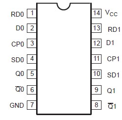
Features: • Metastable immune characteristics• Output skew less than 1.5ns• High source current (IOH = 15mA) ideal for clock driver applications• See 74F5074 for synchronizing dual Dtype flipflop• See 74F50109 for synchronizing dual JK positive edgetriggered flipflop&...
74F50729: Features: • Metastable immune characteristics• Output skew less than 1.5ns• High source current (IOH = 15mA) ideal for clock driver applications• See 74F5074 for synchronizin...
SeekIC Buyer Protection PLUS - newly updated for 2013!
268 Transactions
All payment methods are secure and covered by SeekIC Buyer Protection PLUS.
(Operation beyond the limit set forth in this table may impair the useful life of the device. Unless otherwise noted these limits are over the operating free air temperature range.)
SYMBOL |
PARAMETER |
RATING |
UNIT | |
VCC |
Supply voltage |
0.5 to +7.0 |
V | |
VIN |
Input voltage |
0.5 to +7.0 |
V | |
IIN |
Input current |
30 to +5 |
mA | |
VOUT |
Voltage applied to output in High output state |
0.5 to VCC |
V | |
IOUT |
Current applied to output in Low output state |
40 |
mA | |
Tamb |
Operating free air temperature range | Commercial range |
0 to +70 |
|
Industrial range |
40 to +85 |
|||
Tstg |
Storage temperature range |
65 to +150 |
The 74F50729 is a dual positive edgetriggered Dtype featuring individual data, clock, set and reset inputs; also true and complementary outputs.
The 74F50729 is designed so that the outputs can never display a metastable state due to setup and hold time violations. If setup time and hold time are violated the propagation delays may be extended beyond the specifications but the outputs will not glitch or display a metastable state. Typical metastability parameters for the 74F50729 are: t @ 135ps and t @ 9.8 X 10⁶ sec where t represents a function of the rate at which a latch in a metastable state resolves that condition and To represents a function of the measurement of the propensity of a latch to enter a metastable state.
Set (SDn) and reset (RDn) are asynchronous positiveedge triggered inputs and operate independently of the clock (CPn) input. Data must be stable just one setup time prior to the lowtohigh transition of the clock for guaranteed propagation delays.
Clock triggering of the 74F50729 occurs at a voltage level and is not directly related to the transition time of the positivegoing pulse. Following the hold time interval, data at the Dn input may be changed without affecting the levels of the output.