
Circuit Diagram
Index 315
Telephone Guard circuit
Published:2012/9/28 20:46:00 Author:muriel | Keyword: Telephone Guard

Here is a simple circuit to protect your Telephone, EPBAX, Telephone Modem etc from lightning discharge or line spikes. It uses a safety capacitor and Gas Tube Arrester to prevent damage of the devices
The circuit is too simple but its use is great. The main elements of the circuit are a Gas Discharge Tube (GDT) and a safety capacitor.
Gas Discharge Tube
The GDT used in the circuit is NS2R – 230 A1 – N make 2 pole Arrester. It is a 2 electrode Ceramic Gas Tube Arrester rated 5KA / 5A. GDT is a surge protection device do the same job as an MOV. GDT divert the extra current from the hot line to the ground line using an inert gas as the conductor between the two lines.
When the voltage is at a certain level, the gas inside the GDT remains non conducting. When the voltage surges above that level occurs, the electrical power is strong enough to ionize the gas, making the gas a very effective conductor. It then passes current to the ground line until the voltage reaches normal level. Then again GDT becomes a poor conductor.
2 Electrode GDT
Safety Capacitor
Safety Capacitors are designed to withstand high impulse voltages in applications where human beings might be exposed to voltage surges. These capacitors will shunt the energy from the impulse to ground, protecting the circuit from the surge. Safety capacitors are available in ceramic disc and metalized film or paper. The film type are made of self-healing metalized polyester, polypropylene or paper and usually come in a “box” style casing as the capacitor is encased is a flame retardant or flame-proof case. The safety capacitor used in the circuit is 220 K 250Volt DC
220K 250 V DC Capacitor
The circuit is self explanatory and easy to make on a piece of Perf board.You can also do lead-to-lead soldering. Enclose the circuit in a small box and connect to the telephones lines and phone / modem as shown in the diagram.
Telephone Guard Circuit Diagram
(View)
View full Circuit Diagram | Comments | Reading(750)
Dancing Light circuit
Published:2012/9/28 20:46:00 Author:muriel | Keyword: Dancing Light
Here is a simple Dancing LED Circuit. The LEDs turns on/off alternately giving a dancing appearance. It is a simple Astable multivibrator using two NPN transistors.It works on the principle of charging and discharging of capacitors C1 and C2. Current from the positive of battery flows through first set of LEDs D1-D3 to the collector of T1 through resistor R1. Resistor R1 limits current through the LEDs to protect them. The current through R1 charges capacitor C2. It then discharges through the base of T2 and resistor R4. This gives base current to T2 and it conducts. As a result second set of LEDs D4-D6 lights as the current flows through T1.Capacitor C2 again charges and the cycle repeats.
Dancing Light Circuit
The same thing happens in the other side also. This gives alternate flashing of LEDs. (View)
View full Circuit Diagram | Comments | Reading(1492)
Capacitor Power Supply circuit
Published:2012/9/28 20:46:00 Author:muriel | Keyword: Capacitor, Power Supply
One of the major problems that is to be solved in an electronic circuit design is the production of low voltage DC power supply from Mains to power the circuit. The conventional method is the use of a step-down transformer to reduce the 230 V AC to a desired level of low voltage AC. The most simple, space saving and low cost method is the use of a Voltage Dropping Capacitor in series with the phase line.
Capacitor Power supply Circuit
Selection of the dropping capacitor and the circuit design requires some technical knowledge and practical experience to get the desired voltage and current. An ordinary capacitor will not do the job since the device will be destroyed by the rushing current from the mains. Mains spikes will create holes in the dielectric and the capacitor will fail to work. X-rated capacitor specified for the use in AC mains is required for reducing AC voltage.
X Rated capacitor 400 Volt
(View)
View full Circuit Diagram | Comments | Reading(1194)
Power-saving voltage regulator circuit
Published:2012/9/27 22:23:00 Author:Ecco | Keyword: Power-saving, voltage regulator
The regulator have the funtions of general delay regulator, and its main features are: ( 1) When mains voltage is in 220V ± 10 % safe voltage range, the regulator automatically disconnected from the mains, then the mains is added to the load to eliminate its loss. ( 2) When the mains exceeds safe voltage range, it will be automatic step-up or step-down. ( 3) When the load is zero, the regulator is automatically disconnected from the mains to eliminate the no-load loss. ( 4 ) When input voltage is 160V ~ 270V, output voltage is 220V ± 10% to meet national standards. Power is 2500W.
(View)
View full Circuit Diagram | Comments | Reading(1587)
The switching circuit 1 with self-locking ( self-maintaining ) function
Published:2012/9/27 21:55:00 Author:Ecco | Keyword: switching , self-locking , self-maintaining function
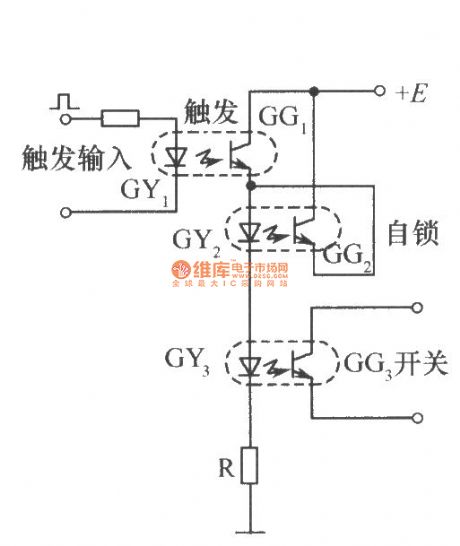
The 3 optical couplers in Figure respectively play the role of the trigger, self-locking and switching. When a start trigger signal is applied to the GY , GG1 gets conduction, then there is current flowing through GY2 and GY3 to turn on GG2 and OG3. When the trigger signal disappears, GY1 does not emit light, then GG1 is cutoff, but at this time, the GG2 has been turned on, and the current of GY2 and GY3 is provided by GG2 passage, GG3 continues to maintain the conductive state, it is equivalent that the switch is still turned on until the power supply voltage E disappears in order to make the circuit restitution.
(View)
View full Circuit Diagram | Comments | Reading(745)
Four gratings circuits using integrated circuit
Published:2012/9/27 21:40:00 Author:Ecco | Keyword: Four , gratings , integrated circuit
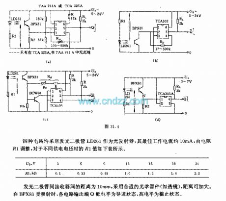
The four circuits use light - emitting diode LD261 as light emitter, and its optimum operating current is about 10mA, and it is adjusted by the resistor R1, the R1 values for the different supply voltages are shown in following table. The distance between the light emitting diode and receiver is 10mm, it uses a suitable optical device ( such as lens ) to increase the distance. When BPX81 is irradiated, each circuit is in turn-on state when output terminal Q is low and off-state when output terminal Q is high.
(View)
View full Circuit Diagram | Comments | Reading(1262)
Grating circuit with Schmitt Trigger
Published:2012/9/27 21:25:00 Author:Ecco | Keyword: Grating , Schmitt Trigger
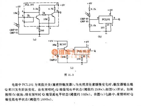
The FCL101 in circuit is a threshold switch (Schmitt trigger), when the illumination changes arbitrarily and slowly, the flip - flop's output terminal Q occurs step change. When there is lighting, the Q end is in low level (threshold is about 250lx ), and it is shown in Figure a. If it is connected like Figure b, the Q terminal is in high level when there is lighting ( threshold value approximately 100lx. In the circuit shown in FIG c, Q-side is in lowlevel (threshold value is approximately 1600lx ).
(View)
View full Circuit Diagram | Comments | Reading(839)
Uniaxial magnetic field sensor with the serial interface ( integrated magnetic field sensor HMC1001)
Published:2012/9/27 21:12:00 Author:Ecco | Keyword: Uniaxial, magnetic field , sensor , the serial interface , integrated
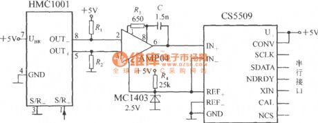
The output stage of the circuit uses a 16-bit A / D converter CS5509 which can be matched with a microprocessor or microcontroller by interface circuit. The AMP04's output voltage (Uo) is connected to CS5509 analog input end, and MC1403 bandgap reference voltage source provides 2.5V reference voltage for CS5509.
(View)
View full Circuit Diagram | Comments | Reading(1842)
Atmospheric Charge Monitor circuit
Published:2012/9/27 21:41:00 Author:muriel | Keyword: Atmospheric, Charge Monitor
This circuit is designed to monitor the atmospheric charge. By observing the increase in the atmospheric charge, it is possible to predict a nearby lightning. The sudden electric discharge during a lightning may cause the flow of excessive current to earth which may be detrimental to the appliances connected to mains lines.Normal atmospheric charge on a sunny day will be around 100 milli volts with negligible current and may increase to many volts as the clouds accumulate in the sky. This may go up to thousands of volts before the lightning strikes. The circuit described here monitors the atmospheric condition and display the same through LED indications.
The front end of the Atmospheric Charge circuit has a Op Amp comparator built around IC TL071. It is a JFET input op amp with an open loop voltage gain of 100dB.Its inverting input is connected to the positive rail through two presets VR1 and VR2 while the non inverting input is connected to the antenna. Resistor R2 protects the input of IC from excessive charge while R1 keeps the non inverting input stable. TL071 has very high gain, so R3 is provided to give some negative feedback.
Output from IC1 is around 2.5 to 5 volts which passes to the input pin5 of IC2 through VR3. Resistor R4 protects VR3 if its wiper is turned fully. IC2 LM3914 is a monolithic integrated circuit< that can sense analogue voltage levels to drive the LEDs and provide a linear analogue display. Current through the LEDs is self regulated by the IC eliminating the need of current limiting LED resistors. Its low bias current input pin5 receives signals down to 0.5 volts and its outputs 18 to 10 sinks current one by one as its input receives an increment of 125 milli volts. The LEDs can give a DOT mode display if pin 9 of IC2 is unconnected. If it is connected to positive rail, bar mode display can be obtained.D1 lights when the input pin 5 gets 1.7 volts andD5 light up when the input gets 4.2 volts.
Atmospheric Charge Monitor Circuit diagram
Adjustments
Before applying power to the circuit, turn the wiper of VR1 to the extreme anti clock position and keep the wiper of VR3 in the middle position. When the wiper of VR2 turns to clock wise direction, D2 to D5 light up one by one. Adjust VR3 till D4 turns on. Wait for some time and see that D5 is glowing. This shows that the circuit is responding to changes in atmospheric charge. It is necessary to make adjustments on a sunny day with clear sky. Adjust VR2 till D1 glows. This indicates normal atmospheric charge. As the charge in the atmosphere increases due to the accumulation of clouds, D2 through D5 lights.
Antenna can be 3 meters plastic wire. The negative rail of the circuit should be earth grounded since the circuit is monitoring the atmospheric potential with reference to ground. Earth grounding can be done by piling an iron rod into the earth. Connect the circuits negative to this iron rod. Keep the unit inside the room near the window. Do not try adjustments if there is lighting. (View)
View full Circuit Diagram | Comments | Reading(934)
Snap Action Relay circuit
Published:2012/9/27 21:40:00 Author:muriel | Keyword: Snap Action, Relay
When a Relay driver circuit is used in Sensor based electronic circuits, false triggering may occurs due to unwanted relay clicking. The input signal level is not sharp in most sensor circuits and the transition stages are slow. So the relay driver transistor partially turns on / off . The relay coil will not become fully energized leading to vibration of the relay contacts and heating. A Snap Action relay driver with Schmitt trigger action can eliminates this.
The diagram below is the relay driver circuit with Snap Action for the clean switching of the relay. When the input signal at the base of T1 decreases, it turns off allowing T2 to conduct by giving base current through R3.When T2 conducts, its emitter current increases and this raises the voltage at the emitter of T1.This rapidly reduces the base current of T1 and it switches off rapidly. When T1 turns off rapidly, T2 turns on faster and relay energize. This snap action reduces the time gap between the working of T1 and T2 and prevents relay chattering.
Snap Action Relay Circuit
Note: The value of R2 must be higher than the resistance of the Relay coil to give more current through R5 when T2 turns on and less flow when T1 turns on. (View)
View full Circuit Diagram | Comments | Reading(839)
Mini Led Flashlight with IC
Published:2012/9/27 21:39:00 Author:muriel | Keyword: Mini, Led, Flashlight
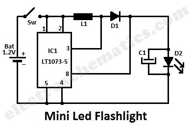
This led lamp circuit can be used as a mini led flashlight. Together with a 1.2 V rechargeable battery, all the components fit into a small enclosure. This is actually a DC to DC converter that convert voltage from a small value to a higher one.The voltage of the battery affects the brightness of a light-emittind diode but if you use this circuit that won’t be a problem anymore. One difference between 1.2 V and 1.5 V is practically not detectable.
The capacitor C1 is used as afterglow when switching off the power supply voltage. If you don’t need this you may disconnect C1. For coil L1 you should use a 82 µH or a 68µH. If you use a lower value for L1 then the circuit will consume more power than really should do.
Although this mini led flashlight kit contains an IC, this circuit is suitable for beginners. This circuit is fast and allows a quick sense of achievement. With a bit of skill to make a case (such as a can or box) is adopted so that this circuit with battery takes place.
Led Flashlight circuit diagram
Components ValuesIC1 = DC-DC converter – LT1073-5L1 = Coil – 82 uHC1 = Capacitor 220 μFD1 = Diode 1N5818D2 = LED / White / Super bright
(View)
View full Circuit Diagram | Comments | Reading(2429)
LED flashing circuit
Published:2012/9/27 21:38:00 Author:muriel | Keyword: LED, flashing circuit
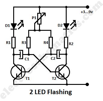
This is a simple led flashing circuit with 2 leds. It illustrates the behavior of transistors and capacitors and if you use an oscilloscope it will be very easy to determine what happens in this astable multivibrator circuit. It’s state is constantly changing and this change affect the flow of current and voltage and the effect will be visible with the two leds.The speed of the led flasher may be adjusted with potentiometer P1. Being an astable multivibrator, the circuit knows no stable state but oscillates continuously between two states back and forth. The two transistors T1 and T2 turn and lock each other by turn. The smaller the capacitor and the smaller the resistance , the faster goes out the appropriate diode, for the benefit of others, who then immediately turns on.
The activation time of T2 is t, a = 0.7 x R1 x C1, the switch-off t off = 0.7 x R2 x C2.
The switch from T1 is t, a = 0.7 x R2 x C2, the off t off = 0.7 x R1 x C1.
The transistors do not necessarily have to be BC 547 B, you may use BC 238 or similar small-signal transistors. It is recommended to always use the equivalent transistors. If one of the transistors is defective, wrong or have a malfunction , so does this to the full functionality of this circuit . An LED lights up and the other only very weakly.
The two led flashing circuit is designed for 9 Volts but it works at even less voltages. In this designed we used red leds but by changing the series resistors R1 and R4 you can also use different colored LEDs.
Two Led flashing circuit diagram
Components valuesR1 - 470 OhmR2 - 470 OhmR3 - 3.9 kOhmR4 – 3.9 kOhmP1 - 50 kOhmC1 – 47 μF / 16VC2 - 47 μF / 16VT1 - BC 547 BT2 - BC 547 BD1 - LED Standard , 5 mm , redD2 - LED Standard , 5 mm , red
(View)
View full Circuit Diagram | Comments | Reading(2537)
78XX Voltage Regulator circuit
Published:2012/9/27 21:37:00 Author:muriel | Keyword: 78XX, Voltage Regulator
IC 78XX Series includes three terminal positive voltage regulators commonly available in TO 220 package. These are useful in wide range of applications to give precise output voltage. These regulators have internal current limiting, and thermal shutdown circuitry etc. If good heat sinking is provided, these ICs can deliver 1 Amps current. These are generally considered as fixed voltage regulators but their functions can be manipulated to convert them into variable voltage regulators78 XX REGULATOR IC
.
The important parameters of 78 XX series are1. Maximum output current 1.5A2. Output voltages – 5,5.2,6,8,9,10,12,15,18,24volts3. Thermal overload protection4. Short circuit protection
The following circuits give an idea about the input voltage at which the IC gives precise output. Fig 1 and 2 shows the conditions in which the IC7805 is giving precise 5 volt output. 7805 IC requires minimum 6.5 volts to give 5 volt output. To monitor this, a Zener and LED are included at the input. Zener voltage is 4.7 volts and the forward voltage drop of the ordinary diffuse type Red LED is 1.8 volts. When the input voltage is above 6.5 volts (4.7+1.8), Zener conducts and LED turn on. This indicates that IC is getting input voltage above 6.5 volts. When the input voltage reduces below 6.5 volts, Zener cut off and LED turns off.
7805 Circuit 1
Fig 2 shows another LED indication. The brightness of LED reduces as the input voltage reduces below 6.5 volts.
(View)
View full Circuit Diagram | Comments | Reading(947)
Power Supply Guard circuit
Published:2012/9/27 21:37:00 Author:muriel | Keyword: Power Supply, Guard
Here is a Power Supply Guard circuit that can be used as a protective device in power supply boxes. This type of Spike protection circuit is present in the multi socket switch boards used to connect computer peripherals. This circuit is useful to guard the electronic or electrical devices from mains transients and spikes. If heavy transients develop in the mains, the MOV in the circuit short circuit the lines and the fuse will blow out.
The Power Supply Guard circuit uses a Metal Oxide Varistor 431KD14, a 0.1 uF X2 rated AC capacitor, a Toroidal transformer and two 2KV disc capacitors.Components:
Metal Oxide Varistor
Metal Oxide Varistor (MOV) contains a ceramic mass of zinc oxide grains, in a matrix of other metal oxides such as small amounts of bismuth, cobalt, manganese etc. sandwiched between two metal plates which forms the electrodes. The boundary between each grain and its neighbour forms a diode junction, which allows current to flow in only one direction. When a small or moderate voltage is applied across the electrodes, only a tiny current flows, caused by reverse leakage through the diode junctions. When a large voltage is applied, the diode junction breaks down due to a combination of thermionic emission and electron tunneling, and large current flows. Varistors can absorb part of a surge.The effect depends on the equipment and details of the selected varistor.
MOV
A varistor remains non-conductive as a shunt mode device during normal operation when voltage remains well below its “clamping voltage”. If a transient pulse is too high, the device may melt, burn, vaporize, or otherwise be damaged or destroyed.
Toroidal TransformerToroidal transformers are built around a ring-shaped core. The primary and secondary coils are often wound concentrically to cover the entire surface of the core. This minimizes the length of wire needed, and also provides screening to minimize the core’s magnetic field from generating electromagnetic interference. In the circuit, the toroidal transformer is made using primary and secondary winding each having 20 turns of 22 SWG enameled copper wire. The core can be procured from the damaged power supply boards of UPS or SMPS.
Power Supply Guard Circuit
Toroidal transformer
Toroid Core
2 KV Capacitor 0.1 uF X rated AC Cap 250 volt
Power supply Guard – Assembled Board
(View)
View full Circuit Diagram | Comments | Reading(851)
Electronic Organ Circuit
Published:2012/9/27 21:37:00 Author:muriel | Keyword: Electronic Organ
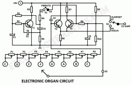
This electronic organ circuit is very simple to construct and is basically an emitter-coupled oscillator composed of T2 and T3. An squarewave voltage can be sampled from the collector of T3 (X2). This signal gives a clarinet character to the tone.Without the squarewave signal, the sound produced by emitters of T2 and T3 (X4) has a violin character. An additional vibrato signal can be added to this basic sound through switch S1. The frequency of the vibrato is around 6 Hz. Its amplitude is determined by the R4. The value of R4 can vary from 100 up to 300KΩ but you can experiment with different values.
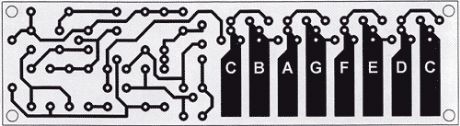
The organ keys can be made of either metal plates or etched printed circuit.The trimmers P1 up to P8 adjust the pitch of each tone. The tones can be drastically changed by changing the value of C4.
Electronic Organ circuit diagram
Printed Circuit Board for the Electronic Organ
(View)
View full Circuit Diagram | Comments | Reading(2365)
LED VoltMeter circuit
Published:2012/9/27 21:36:00 Author:muriel | Keyword: LED, VoltMeter
Here is a Simple LED Voltmeter to Monitor the charge level in Lead Acid Battery or Tubular battery. The terminal voltage of the battery is indicated through a four level LED indicators.The nominal terminal voltage of a Lead Acid battery is 13.8 volts and that of a Tubular battery is 14.8 volts when fully charged. The LED voltmeter uses four Zener diodes to light the LEDs at the precise breakdown voltage of the Zener diodes. Usually the Zener diode requires 1.6 volts in excess than its prescribed value to reach the breakdown threshold level. When the battery holds 13.6 volts or more, all the Zener breakdown and all LEDs light up. When the battery is discharged below 10.6 volts, all the LEDs remain dark. So depending on the terminal voltage of the battery, LEDs light up one by one or turns off.
LED VoltMeter Circuit Schematic
(View)
View full Circuit Diagram | Comments | Reading(804)
Battery Self discharge Indicator
Published:2012/9/27 21:36:00 Author:muriel | Keyword: Battery, Self discharge, Indicator
If the lead acid battery is not using for long time, self discharge takes place at the rate of 4 % per week at 27 degree. For example, a 125 Ah tubular battery self discharge at the rate of 5 Amps current per week if it is not in charge / discharge cycles. This add on circuit can be used to detect the self discharge of the 12 volt lead acid battery below the safe level of 11.6 volts. It is ideal to monitor the charge level in the battery, it the battery is not using for long period.The Battery Self discharge Indicator circuit uses only a few components and its working is simple. A PNP transistor T1 act as a switch to light the LED, if the battery voltage drops below the safe level. The base bias of T1 is controlled by a Zener diode ZD. Its rating is 10 volt 1 W. The Zener diodes usually requires 1.6 volts excess than its rated value to enter into the “Avalanche state”.
Battery Self discharge Indicator Circuit
So, as long as the battery voltage is above 11.6 (10+1.6), Zener conducts and keeps the base of T1 high. Since T1 is a PNP transistor, it will not conduct till its base becomes negative. So LED remains dark. When the voltage in the battery reduces below 11 volts, Zener turns off and the base of T1 becomes negative. T1 then conducts and LED lights. So the battery can be charged again to keep it in top condition. Preset VR can be used to set the exact point at which LED turns on. (View)
View full Circuit Diagram | Comments | Reading(779)
FSK Filter circuit
Published:2012/9/27 21:35:00 Author:muriel | Keyword: FSK Filter
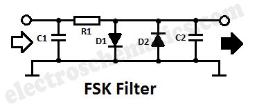
FSK or Frequency-Shift Keying is a form of frequency modulation in which the modulating signal shifts the output freq. between predetermined values. If problems arise in demodulating FSK signals, it is helpful to use the FSK filter circuit presented here. The Frequency-Shift Keying filter is very simple and it can be built inside a phone plug. The diagram shows a low pass filter made of R1 and C2. This filter has a cutoff freq. of about 1.6 KHz. Since the “0″ and “1″ signals of the FSK are sent as tones of 1.2 KHz and 2.4 KHz respectively, the filter removes all unwanted corners fron the signal.
Both D1 and D2 ensure that the FSK signal is limited to about +/- 600 mV amplitude. It can be attached to a loudspeaker or headphone output.
FSK Filter circuit diagram
Components valuesC1 = 0.0082C2 = 0.018R1 = 5.6kΩD1 = D2 = 1N4148 (View)
View full Circuit Diagram | Comments | Reading(1324)
FM Stereo Noise Suppressor
Published:2012/9/27 21:34:00 Author:muriel | Keyword: FM, Stereo, Noise Suppressor

This fm stereo noise suppressor circuit is to be used when the reception of far FM stations is bad but improves when you switch the radio receiver to mono. The cause of this effect is that in stereo reception the biggest part of the noise in the right channel is in opposite phase with the noise in the left channel. Once the 2 channels are switched togheter (mono), the noise signals cancel each other and the result will be a clean and relatively noise free mono signal.
In order to use this effect in improving the signal but keeping the stereo character, the two channels should be switched together only in higher audio frequencies.
The stereo noise suppressor circuit is built in 2 identical channels each composed of 2 emitter-follower circuits. The switch S1 (single throw/3 poles switch) can connect the 2 channels together at 3 points. The circuit functions as a bridge between the left and right channel for opposing signal components above 8 kHz. These signals get “short-circuited” cancelling the noise. Otherwise, all other frequencies get through to the output via their respective channels.
If you want to lower the “short-circuit” freq. to 4 kHz, just double the values of C2, C3 and C4.T1 = T2 = 2SC734
FM Stereo Noise Suppressor circuit diagram
(View)
View full Circuit Diagram | Comments | Reading(1573)
Heatsink temperature monitor circuit
Published:2012/9/27 21:33:00 Author:muriel | Keyword: Heatsink, temperature monitor

This heatsink temperature monitor circuit signals via 3 LEDs when the temperature exceeds 2 boundary levels. When the heatsink temperature is below 50 … 60oC (122 … 140oF) the greed LED lights. The yellow one signals that the temperature is within 60 and 70oC (140 … 158oF). The red one signals that the temperature has reached beyond 70 … 80o (158 … 176oF). At this point a relay can be triggered to break the power supply or otherwise protect the electronic device by turning ON a cooling fan.
As shown in the circuit diagram the heatsink monitor is made of 2 opamps that are set as window comparators. The input voltage level is set by the thermosensor IC LM335. This voltage level increses linearly by a factor of 10mV/oC. If this voltage is below the voltage level set by P1 and P2, the opamp outputs are almost at ground potential (0V) and the green LED lights up.
To set the desired temperature levels: put the thermosensor LM355 together with a thermometer into a pot of water which is being heated slowly. Turn P1 to its lowest point and turn P2 to its maximum. The switching point from green LED to yellow (50 … 60oC) is set with P1. The switching point from yellow to red is set withh P2. Watch thermometer while the water is being heated and adjust the potentiometers accordingly. Once the desired values are set, attach the thermosensor to the heatsink.
Heatsink Monitor circuit diagram
(View)
View full Circuit Diagram | Comments | Reading(2086)
| Pages:315/2234 At 20301302303304305306307308309310311312313314315316317318319320Under 20 |
Circuit Categories
power supply circuit
Amplifier Circuit
Basic Circuit
LED and Light Circuit
Sensor Circuit
Signal Processing
Electrical Equipment Circuit
Control Circuit
Remote Control Circuit
A/D-D/A Converter Circuit
Audio Circuit
Measuring and Test Circuit
Communication Circuit
Computer-Related Circuit
555 Circuit
Automotive Circuit
Repairing Circuit