
Circuit Diagram
Index 196
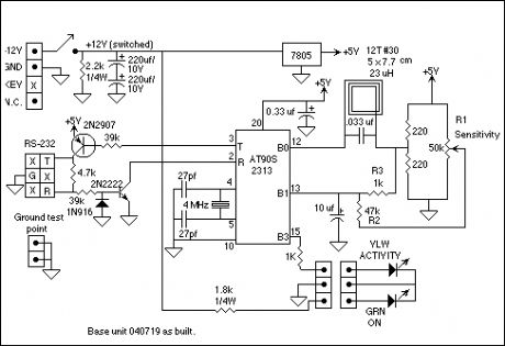
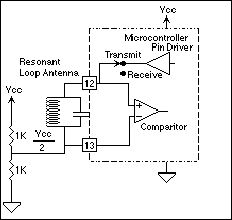
Minimum Mass Wireless Coupler Terminal Interface
Published:2013/1/22 20:45:00 Author:muriel | Keyword: Minimum Mass , Wireless Coupler, Terminal Interface
View full Circuit Diagram | Comments | Reading(596)
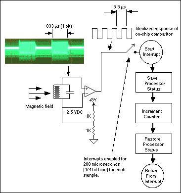
The receiver
Published:2013/1/22 20:44:00 Author:muriel | Keyword: receiver
View full Circuit Diagram | Comments | Reading(739)
transmitter sends on-off keyed serial data
Published:2013/1/22 20:44:00 Author:muriel | Keyword: transmitter, on-off keyed , serial data

View full Circuit Diagram | Comments | Reading(1236)
Minimum Mass Wireless Coupler
Published:2013/1/22 20:43:00 Author:muriel | Keyword: Minimum Mass, Wireless Coupler
View full Circuit Diagram | Comments | Reading(590)
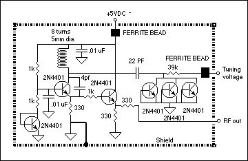
90 MHz VFO for Frequency Modulation
Published:2013/1/22 20:43:00 Author:muriel | Keyword: 90 MHz , VFO, Frequency Modulation
View full Circuit Diagram | Comments | Reading(1260)
100 MHz frequency source
Published:2013/1/22 20:42:00 Author:muriel | Keyword: 100 MHz , frequency source
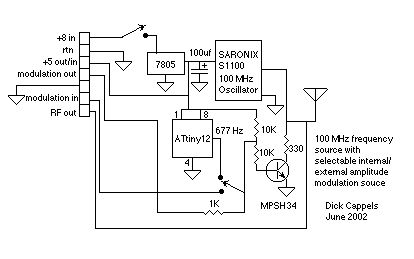
View full Circuit Diagram | Comments | Reading(580)
1.5V Battery operated FM rebroadcast transmitter
Published:2013/1/22 20:42:00 Author:muriel | Keyword: 1.5V Battery , operated, FM rebroadcast , transmitter

View full Circuit Diagram | Comments | Reading(801)
FM Broadcast Audio Transmitter
Published:2013/1/22 20:41:00 Author:muriel | Keyword: FM Broadcast , Audio Transmitter
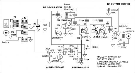
View full Circuit Diagram | Comments | Reading(865)
Low Power PLL FM Transmitter
Published:2013/1/22 20:38:00 Author:muriel | Keyword: Low Power, PLL, FM , Transmitter

View full Circuit Diagram | Comments | Reading(1327)
VFC121V / F converter application temperature measurement system
Published:2013/1/22 2:40:00 Author:Ecco | Keyword: converter application , temperature measurement system
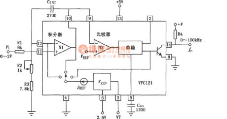
VFC121 uses high-frequency NPN / PNP charge balance technology to realize V / F conversion, and its power supply is flexible( 4.5 to 36V), and the voltage output is proportional to absolute temperature, thus it can be used as the system environment temperature measurement for D / A converters, data acquisition and system deviating occasion. VFCl21 uses 0IP 14-pin double-row arrangement package, and its pinout and internal circuit block diagram is shown as below.
(View)
View full Circuit Diagram | Comments | Reading(1012)
The ICS1523 Typical Application Circuit
Published:2013/1/22 2:51:00 Author:Ecco | Keyword: Typical Application

The circuit provides the video sync signal for SIDl3806 display controller. These signals are required by SIDl3806 connecting LCD. ICSl523 input clock is 50 MHz ( pin 12 ), the output is CLKl ( 25 MHz), CLK2 (12.5 MHz ) and CLK3 (387.6 kHz), and they are respectively connected to S1D13806 BUSCLK ( pin 60 ), CLKl ( pin 66 ) , CLKl2 ( pin 64 ) and CLKl3 ( pin ).
(View)
View full Circuit Diagram | Comments | Reading(611)
HDAC7542 12 - bit parallel port D / A converter
Published:2013/1/22 2:48:00 Author:Ecco | Keyword: 12 - bit, parallel port, D / A converter

HDAC7542 can be directly matched with CPU, and it is a low-power, high-speed, high - gain 12-bit multiplying D / A converter. The digital signal is divided into 3 groups which is input tp memory by 4 bytes, and its internal data is written to the D / A converter after passing cache twice, then the D / A converter output is updated for four-quadrant multiplication. Its typical application circuit is shown as figure. Figure (A) shows the unipolar 2-quadrant multiplying connection.
(View)
View full Circuit Diagram | Comments | Reading(1162)
MC1420/1520 wideband op amp and its pin main characteristics
Published:2013/1/22 1:32:00 Author:Ecco | Keyword: wideband op amp , pin main characteristics
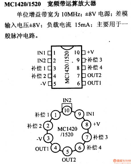
The unity-gain bandwidth is 10MHz; differential-mode input voltage is ± 8V; load current is 15mA; it is mainly used for general pulse circuit.
(View)
View full Circuit Diagram | Comments | Reading(824)
MC14573 quad CMOS programmable operational amplifier and its pin main characteristics
Published:2013/1/22 1:55:00 Author:Ecco | Keyword: quad CMOS, programmable, operational amplifier, pin main characteristics
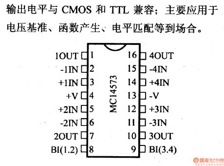
The power supply is -0.5 ~ +18 V; the input Voltage is -0.5 ~~ V +0.5 V; input current (DC ) is 10mA; operating voltage can be as low as ± 1.5V; output level is compatible with CMOS and TTL; it is mainly used in voltage reference, function generator and level matching occasions.
(View)
View full Circuit Diagram | Comments | Reading(840)
MC1437/1537 double-pass op amp and its pin main characteristics
Published:2013/1/21 0:29:00 Author:Ecco | Keyword: double-pass op amp , pin main characteristics
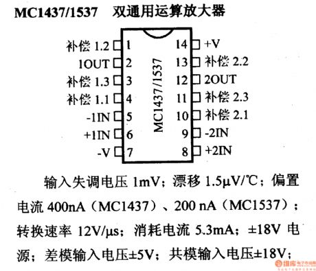
1mV input offset voltage; 1.5μV/℃ drift; bias current is 400nA ( MC1437 ) or 200nA ( MC1537 ; conversion rate is 12V/μs; Current consumption is 5.3mA; power supply is ± 18V; differential-mode input voltage is ± 5V; common-mode input voltage is ± 18V; power consumption is 625mW.
(View)
View full Circuit Diagram | Comments | Reading(1149)
NE538 high - speed operational amplifier and its pin main characteristics
Published:2013/1/21 0:36:00 Author:Ecco | Keyword: high - speed, operational amplifier, pin main characteristics
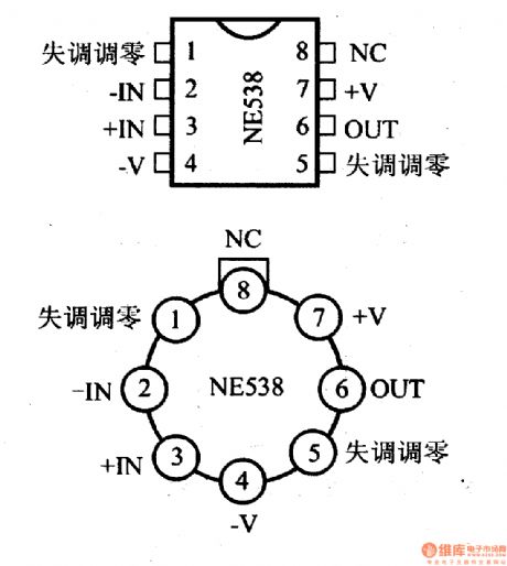
Input offset voltage is 2mV; temperature drift is 6μV / ℃; bias current is 65nA; Gain Bandwidth Product GB = 6MHz; conversion rate is 60V/μs; noise is 30nV / √ ¯ Hz (1kHz); Current consumption is 2mA; power supply is ± 18V; differential-mode input voltage is ± 30V; common-mode input voltage is ± 15V; power is 800mW.
(View)
View full Circuit Diagram | Comments | Reading(806)
NE5532 / A dual low-noise op amp and its pin main characteristics
Published:2013/1/21 0:41:00 Author:Ecco | Keyword: dual low-noise op amp , pin main characteristics
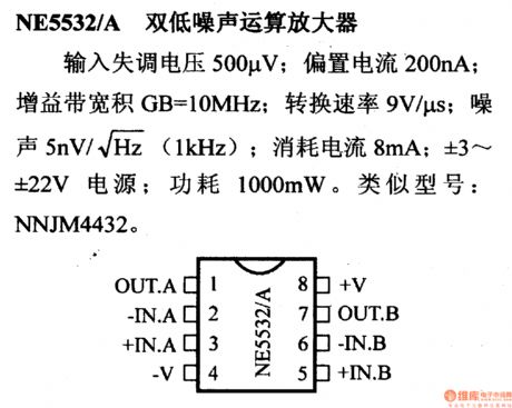
Input offset voltage is 500μV; bias current is 200nA; Gain Bandwidth Product GB = 10MHz; conversion rate is 9V/μs; noise is 5nV / √ ¯ Hz ( 1kHz); Current consumption is 8mA ; ± 3 to ± 22V power supply; power is 1000mW. Similar models: NNJM4432.
(View)
View full Circuit Diagram | Comments | Reading(2549)
NE5534 / A low-noise op amp and its pin main characteristics
Published:2013/1/21 0:45:00 Author:Ecco | Keyword: low-noise op amp , pin main characteristics
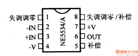
Input offset voltage is 500μV; temperature drift is 4μV / ℃; bias current is 400nA; Gain Bandwidth Product GB = 10MHz; conversion rate is 13V/μs; noise is 3.5nV / √ ¯ Hz ( 1kHz); Current consumption is 4.5mA; ± 3 ~ ± 22V power; power is 800mW.
(View)
View full Circuit Diagram | Comments | Reading(1470)
NJM2043 dual low-noise op amp and its pin main characteristics
Published:2013/1/21 0:49:00 Author:Ecco | Keyword: dual low-noise , op amp , pin main characteristics
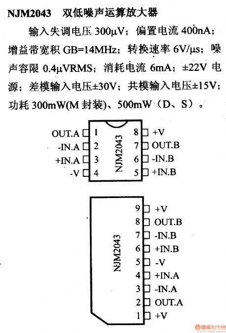
Input offset voltage is 300μV; bias current is 400nA; Gain Bandwidth Product GB = 14MH ; conversion rate is 6V/μs; noise is 0.4μVRMS; Current consumption is 6mA; power supply is ± 22V; differential-mode input voltage is ± 30V; common-mode input voltage is ± 15V; reactive consumption is 300mW (M package ), 500mW ( D , S ).
(View)
View full Circuit Diagram | Comments | Reading(1150)
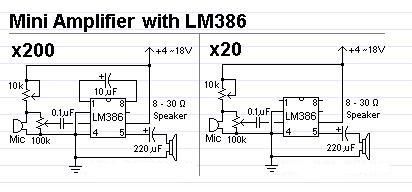
Mini Amplifier with LM386
Published:2013/1/21 0:39:00 Author:muriel | Keyword: Mini Amplifier, LM386
View full Circuit Diagram | Comments | Reading(2215)
| Pages:196/2234 At 20181182183184185186187188189190191192193194195196197198199200Under 20 |
Circuit Categories
power supply circuit
Amplifier Circuit
Basic Circuit
LED and Light Circuit
Sensor Circuit
Signal Processing
Electrical Equipment Circuit
Control Circuit
Remote Control Circuit
A/D-D/A Converter Circuit
Audio Circuit
Measuring and Test Circuit
Communication Circuit
Computer-Related Circuit
555 Circuit
Automotive Circuit
Repairing Circuit