
Circuit Diagram
Index 171
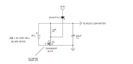
High Power GaAs FET Amplifier 2
Published:2013/2/20 21:04:00 Author:muriel | Keyword: High Power, GaAs FET Amplifier

View full Circuit Diagram | Comments | Reading(841)
High Power GaAs FET Amplifier
Published:2013/2/20 21:03:00 Author:muriel | Keyword: High Power, GaAs FET Amplifier

View full Circuit Diagram | Comments | Reading(840)
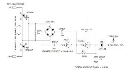
Converting GaAs FET Model 3
Published:2013/2/20 21:03:00 Author:muriel | Keyword: Converting GaAs FET Model

View full Circuit Diagram | Comments | Reading(515)
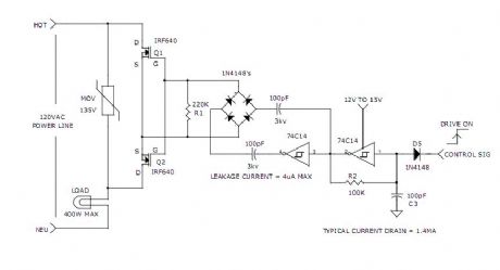
Converting GaAs FET Model 2
Published:2013/2/20 21:02:00 Author:muriel | Keyword: Converting GaAs FET Model

View full Circuit Diagram | Comments | Reading(569)
Converting GaAs FET Model
Published:2013/2/20 21:01:00 Author:muriel | Keyword: Converting GaAs FET Model

View full Circuit Diagram | Comments | Reading(602)
CIRCUIT PROTECTS FROM BATTERY POLARITY REVERSAL 2
Published:2013/2/20 21:00:00 Author:muriel | Keyword: CIRCUIT PROTECTS, BATTERY POLARITY REVERSAL
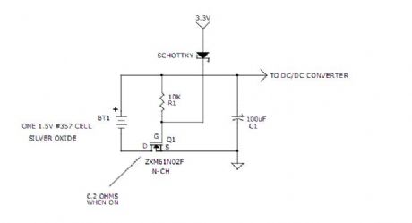
View full Circuit Diagram | Comments | Reading(588)
Charge Coupled MOSFET Relay 1
Published:2013/2/20 20:59:00 Author:muriel | Keyword: Charge Coupled , MOSFET Relay

View full Circuit Diagram | Comments | Reading(681)
CHARGE COUPLED MOSFET RELAY CIRCUIT
Published:2013/2/20 20:57:00 Author:muriel | Keyword: CHARGE COUPLED, MOSFET RELAY

View full Circuit Diagram | Comments | Reading(828)
A better MOSFET H Bridge Schematic
Published:2013/2/20 20:56:00 Author:muriel | Keyword: MOSFET , H Bridge

View full Circuit Diagram | Comments | Reading(1487)
Basic MOSFET/EPAD MOSFET Diode-Connected Circuit
Published:2013/2/20 20:55:00 Author:muriel | Keyword: Basic MOSFET/EPAD, MOSFET, Diode-Connected Circuit

View full Circuit Diagram | Comments | Reading(2150)
Basic MOSFET/ EPAD MOSFET Inverter Circuit
Published:2013/2/20 20:54:00 Author:muriel | Keyword: Basic MOSFET/ EPAD, MOSFET, Inverter Circuit

View full Circuit Diagram | Comments | Reading(835)
Basic EPAD MOSFET Connection with Current Source Drive
Published:2013/2/20 20:53:00 Author:muriel | Keyword: Basic EPAD MOSFET, Connection , Current Source Drive

View full Circuit Diagram | Comments | Reading(646)
REVERSED BATTERY POLARITY PROTECTION CIRCUIT
Published:2013/2/20 20:46:00 Author:muriel | Keyword: REVERSED BATTERY , POLARITY PROTECTION CIRCUIT
View full Circuit Diagram | Comments | Reading(904)
CHARGE PUMP VOLTAGE DIVIDER
Published:2013/2/20 20:45:00 Author:muriel | Keyword: CHARGE PUMP , VOLTAGE DIVIDER

View full Circuit Diagram | Comments | Reading(1392)
Charge Coupled MOSFET Relays
Published:2013/2/20 20:44:00 Author:muriel | Keyword: Charge Coupled, MOSFET Relays
View full Circuit Diagram | Comments | Reading(613)
CHARGE COUPLED BI-DIRECTIONAL POWER MOSFET RELAY
Published:2013/2/20 20:42:00 Author:muriel | Keyword: CHARGE COUPLED , BI-DIRECTIONAL , POWER MOSFET RELAY
View full Circuit Diagram | Comments | Reading(829)
Sample-and-hold amplifier circuit with SMP04 op amp and 10 gain
Published:2013/2/20 0:25:00 Author:Ecco | Keyword: Sample-and-hold , amplifier , op amp , 10 gain
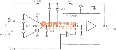
The circuit will place SMP04 in the feedback loop of op amp OP490, when S Non / H = 0, OP490 feedback loop is turned off, SMP04 internal switch is closed, the op amp gain of the circuit is decided by the op-amp and the feedback resistor, the gain in figure is set to 10, the output terminal outputs the amplified sampled voltage. When S non / H = 1, SMP04 internal switch is turned off, the op amp OP490 feedback loop can not form.
(View)
View full Circuit Diagram | Comments | Reading(1483)
Current source circuit with offset compensation in LOG102 input end with OPA335 op amp and the reference voltage source REF3025
Published:2013/2/20 0:38:00 Author:Ecco | Keyword: Current source , offset compensation , LOG102 input end , op amp , reference voltage source
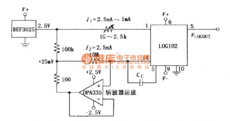
This circuit uses a 1GΩ ~ 2.5kΩ potentiometer to match 2.5nA ~ 1mA reference voltage source and generate the reference current, and it uses low offset chopper op amp OPA335 to compensate input offset voltage, constituting the current source circuit with offset compensation.
(View)
View full Circuit Diagram | Comments | Reading(1420)
Laser diode driver circuit with double broadband transconductance operational amplifier OPA2662
Published:2013/2/20 1:00:00 Author:Ecco | Keyword: Laser diode driver , double broadband, transconductance , operational amplifier
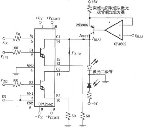
The circuit has a pair of laser -emitting diodes and laser receiver diodes, constituting the reflection laser transmitter and receiver circuits, the figure mainly shows a laser emitting driving circuit.
(View)
View full Circuit Diagram | Comments | Reading(2616)
Analog - digital video tape recording amplifier circuit with double broadband transconductance operational amplifier OPA2662
Published:2013/2/20 1:03:00 Author:Ecco | Keyword: Analog - digital , video tape recording , amplifier , double broadband , transconductance , operational amplifier

Data equalization signal input OPA2662 uses its internal dual OTA to constitute the push-pull output, and its load is the analog - digital video head, the signal is recorded on the tape by the head.
(View)
View full Circuit Diagram | Comments | Reading(1422)
| Pages:171/2234 At 20161162163164165166167168169170171172173174175176177178179180Under 20 |
Circuit Categories
power supply circuit
Amplifier Circuit
Basic Circuit
LED and Light Circuit
Sensor Circuit
Signal Processing
Electrical Equipment Circuit
Control Circuit
Remote Control Circuit
A/D-D/A Converter Circuit
Audio Circuit
Measuring and Test Circuit
Communication Circuit
Computer-Related Circuit
555 Circuit
Automotive Circuit
Repairing Circuit