Power-Supply Circuits-Fixed
Index 6
4.5 to 34V lA adjustable regulated power supply circuit composed of LM105 and integrated power management LM195
Published:2011/5/9 22:17:00 Author:Rebekka | Keyword: integrated power management, adjustable regulated power supply
View full Circuit Diagram | Comments | Reading(593)
15V adjustable regulated power supply circuit composed of μA723
Published:2011/5/9 22:35:00 Author:Rebekka | Keyword: 15V adjustable regulated power supply
View full Circuit Diagram | Comments | Reading(575)
2 to 35V 10A adjustable regulated power supply circuit composed of μA723
Published:2011/5/9 22:34:00 Author:Rebekka | Keyword: 2 to 35V 10A adjustable regulated power supply
View full Circuit Diagram | Comments | Reading(621)
Trimming dual regulated power supply circuit compoed of LM109 and LM120
Published:2011/5/9 22:32:00 Author:Rebekka | Keyword: Trimming dual regulated power supply
View full Circuit Diagram | Comments | Reading(621)
±15V 1A symmetry regulated power supply circuit composed of LM340K-15
Published:2011/5/9 22:15:00 Author:Rebekka | Keyword: symmetry regulated power supply
View full Circuit Diagram | Comments | Reading(959)
Multiple regulated power supply circuit composed of LM309K
Published:2011/5/9 22:11:00 Author:Rebekka | Keyword: Multiple regulated power supply
View full Circuit Diagram | Comments | Reading(800)
10V 2A regulated power supply circuit composed of SG52104
Published:2011/5/9 22:10:00 Author:Rebekka | Keyword: 10V 2A regulated power supply
View full Circuit Diagram | Comments | Reading(587)
13V regulated power supply circuit diagram composed of μ7812
Published:2011/5/9 21:53:00 Author:Rebekka | Keyword: 13V regulated power supply
View full Circuit Diagram | Comments | Reading(794)
Dual regulated power supply circuit composed of LM309K
Published:2011/5/9 21:59:00 Author:Rebekka | Keyword: Dual regulated power supply
View full Circuit Diagram | Comments | Reading(3048)
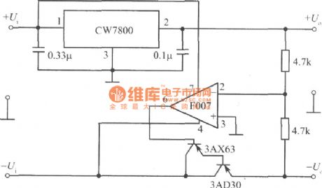
Tracking integrated regulated power supply circuit composed of CW7800 and F007
Published:2011/5/9 4:29:00 Author:Rebekka | Keyword: Tracking integrated regulated power supply

Tracking integrated regulated power supply circuit composed of CW7800 and F007. (View)
View full Circuit Diagram | Comments | Reading(573)
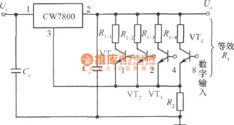
CNC integrated regulated power supply circuit diagram
Published:2011/5/9 4:35:00 Author:Rebekka | Keyword: CNC integrated regulated power supply

CNC integrated regulated power supply circuit diagram. (View)
View full Circuit Diagram | Comments | Reading(634)
PQl2RF2 controllable voltage regulator integrated circuit diagram
Published:2011/5/5 9:49:00 Author:Rebekka | Keyword: Controllable voltage regulator integrated circuit

PQ12RF2 is a controllable voltage regulator integrated circuit. It is widely used in equipment such as species of large screen color TV in the liver. PQ12RF2 integrated circuit IC uses 4-pin single row package, the pin functions and data of the integrated circuit are listed in table 1. (View)
View full Circuit Diagram | Comments | Reading(562)
± 15V and ± 26V output power supply circuit diagram
Published:2011/4/29 1:57:00 Author:Rebekka | Keyword: output power supply

± 15V and ± 26V output power supply circuit diagram is shown as above. (View)
View full Circuit Diagram | Comments | Reading(533)
Using TDA as positive and negative regulator dual power supply circuit diagram
Published:2011/4/28 1:36:00 Author:Rebekka | Keyword: positive and negative , regulator dual power supply

Using TDA as positive and negative regulator dual power supply circuit diagram is shown as above. (View)
View full Circuit Diagram | Comments | Reading(3462)
Using TDA as positive and negative voltage single-supply circuit diagram
Published:2011/4/27 3:49:00 Author:Rebekka | Keyword: positive and negative voltage , single-supply

Using TDA as positive and negative voltage single-supply circuit diagram is shown as above. (View)
View full Circuit Diagram | Comments | Reading(790)
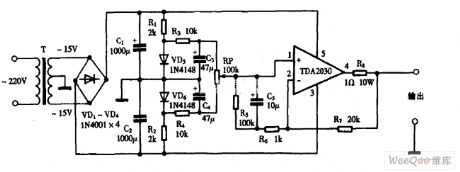
Using TDA2030 as DC power supply circuit diagram
Published:2011/4/27 3:44:00 Author:Rebekka | Keyword: DC power supply circuit

Using TDA2030 as DC power supply circuit diagram is shown as above. (View)
View full Circuit Diagram | Comments | Reading(5487)
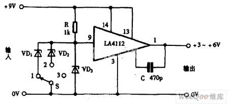
Using LA4112 as regulated power supply circuit diagram
Published:2011/4/26 3:19:00 Author:Rebekka | Keyword: regulated power supply

Using LA4112 as regulated power supply circuit diagram is shown as above. (View)
View full Circuit Diagram | Comments | Reading(1092)
Using LB1405 as DC power supply circuit diagram
Published:2011/4/26 3:14:00 Author:Rebekka | Keyword: DC power supply

Using LB1405 as DC power supply circuit diagram is shown as above. (View)
View full Circuit Diagram | Comments | Reading(1117)
Composed of BIC1222 DC converter circuit diagram
Published:2011/4/25 5:01:00 Author:Rebekka | Keyword: DC converter

Figure 22 is a DC converter circuit constituted by the BIC1222. BIC1222 has two synchronous rectifier power MOSFET, the control circuit, over-current protection circuit and thermal protection circuit module. It has on and off function. The circuit's input voltage is +8 ~ +20 V, output voltage is + 2.5 ~ +5.3 V, output current is 5A. The output voltage is setted by external resistors R1 and R2 in the range of +2.5 ~ +12 V. Output voltage U. = [2.45V (R1 +2 R)] / R2. In the circuit, R2 = 2.2KΩ, U. = 2.5V, R1 = 47Ω; U. 3.3V, R1 = 770Ω; U. 5.0V, R1 = 2.3KΩ. (View)
View full Circuit Diagram | Comments | Reading(743)
INA103 Adjustable Offset Voltage Circuit
Published:2011/4/21 8:01:00 Author:Robert | Keyword: Adjustable Offset Voltage

INA103 Adjustable Offset Voltage Circuit is shown below:
(View)
View full Circuit Diagram | Comments | Reading(698)
| Pages:6/14 1234567891011121314 |
Circuit Categories
power supply circuit
Amplifier Circuit
Basic Circuit
LED and Light Circuit
Sensor Circuit
Signal Processing
Electrical Equipment Circuit
Control Circuit
Remote Control Circuit
A/D-D/A Converter Circuit
Audio Circuit
Measuring and Test Circuit
Communication Circuit
Computer-Related Circuit
555 Circuit
Automotive Circuit
Repairing Circuit


