Light Control
Index 3
PHASE_CONTROLLED_DIMMER
Published:2009/6/17 2:05:00 Author:May

A phase-controlled dimmer delays the triac VAC tum-on to a selected point in each successive ac half cycle. Use this circuit only for incandescent lamps, heaters, soldering irons, or “universal” motors that have brushes. (View)
View full Circuit Diagram | Comments | Reading(3)
HOLIDAY_LIGHT_SEQUENCER
Published:2009/6/17 1:59:00 Author:May

Integrated circuit UI (a 555 oscillator/timer) is wired as a conventional pulse generator. The fre-quency of the pulse generator is controlled by potentiometer R11. Resistor R2 puts a reasonable limit on the highest speed attainable.The output of the pulse generator is fed to the common clock input of U2, a 74C175 quad D-type flip-flop. Each flip-flop is configured so that its Q output is coupled to the D input of the subsequent flip-flop.Information on the D input of each flip-flop is transferred to the Q (and Q) outputs on the lead-ing edge of each clock pulse. Switch 52 allows you to invert the information on the D input of the first flip-flop at any time during the cycle. This allows you to create a number of different sequences, which are determined by the state of the CQ output at the time of the switching.Some of the possible sequences are:· 1 through 4 on, 1 through 4 off;· 1 of 4 on sequence;· 1 of 4 off sequence;· 2 of 4 on sequence;· 1 and 3 on to 2 and 4 off;· and other instances when the sequence of events is difficult to determine.However, if 52 is switched to position B while all outputs are high or all are low (which seldom occurs), the sequence stops and the outputs remain either all on or all off. If that happens, you only need to switch back to position A for at least one pulse duration, then back to position B again.Likewise, S2 should be in position A (pin 4 connected to pin 14) each time the power is turned on. This is because the data on pin 4 must be a logic 1 in order to start a sequence; otherwise all out-puts remain at logic 0, regardless of the clock pulses.Each output of the sequencing circuit is connected to an MOC3010 optoisolator/coupler (U3 through U6), which contains an infrared-emitting diode with an infrared-sensitive diac (triac driver or trigger) in close proximity. The diac triggers the triac, which carries the 117-volts ac.Each time that the infrared-emitting diode receives a logic 1, it turns on and causes the diac to conduct. With the o(Itoisolator/coup ler's internal diac conducting, the triac turns on, and power is supplied to whatever load is plugged into the corresponding ac socket. So, the sequencing circuit and the 117-V ac outputs are optically coupled and are effectively isolated from each other.Power for the sequencing circuit is provided by a 6.3-V miniature transformer. The output of the transformer is rectified by a four-diode bridge circuit, the output of which is filtered by C1 (1000-pF electrolytic capacitor). Capacitor C3 is added at the supply pin of U2 to suppress transients. (View)
View full Circuit Diagram | Comments | Reading(1772)
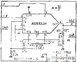
The division circuit for ratio calculation
Published:2011/7/14 23:04:00 Author:Fiona | Keyword: ratio calculation


Circuit function
This circuit is the division circuit that the input signal Z is divided by X. Besides operating EO = 10Z / (-X) and calculating the ratio or percentage,it also can be used as AGC amplifier (A=1/X) which inputs control voltage from the X side. But it can't do large-scale operations. If the input X as the denominator turns smaller, 1 / X will increase,.When X = 0, the gain is infinite, so for division, the range is limited.
Circuit work
If the IC is used as a multiplication, the output voltage feedbacks to the Y input, does the 1 / X calculation, and then multiplies by Z. Because of adding a multiplication unit in the OP amplifier feedback loop, the X input turns smaller so that the circuit would become unstable. and the X values are different, closed-loop frequency characteristics will change because of X's different values. Pay attention to use it.
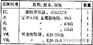
Z-ended input signal has been inverted in the output, the X input only can use the negative voltage . When X = 10V,the circuit uses VR2 to adjust scaling factor to make A = 1. It also can use VR2 to do disorders adjustment of dynamic range of the division circuit.After reducing the variable range, in order to facilitate adjustment, it addsvoltage divider circuit composed of the R1, R2. Input 1V from Z,input 1V from X, adjust VR1 to make the output to be -10V (A =- 10).when Z = 0.1V, X =- 0.1V,it also can get 10V output, but it can not guarantee the accuracy and stability Degrees. In addition, the frequency response changes with the value which is inputed from X.This point also should be noted. (View)
View full Circuit Diagram | Comments | Reading(623)
Outdoor Lighting Automatic Control Principle Circuit
Published:2011/7/18 9:35:00 Author:Robert | Keyword: Outdoor, Lighting, Automatic, Control, Principle

The picture shows the outdoor lighting automatic control principle circuit. (View)
View full Circuit Diagram | Comments | Reading(991)
4-quadrant multiplication analog multiplication arithmetic circuit
Published:2011/7/8 3:20:00 Author:Fiona | Keyword: 4-quadrant multiplication, analog multiplication


Circuit function
MC1494L is a monolithic analog multiplication IC composed of double-balanced differential amplifier, voltage - current converter circuit,a the general multiplication circuit which can use an external device to set the working conditions. It is capable of 4-quadrant multiplication and it is suitable of the various circuit which the input voltage is the positive and negative 10V.
Circuit work
In order to scale factor of 10, the resistances of resistors R5, R6 take 30K and 62K, lead terminal 14 is the collector output type.Owing to the current output,it adds the OP amplifier A1 to convert between current and voltage.The bias of IC1 output becomes the A1's positive input.
(View)
View full Circuit Diagram | Comments | Reading(1017)
absolute value amplifier with polarity detector circuit
Published:2011/6/12 21:36:00 Author:chopper | Keyword: absolute value amplifier, polarity detector
View full Circuit Diagram | Comments | Reading(552)
LCD Backlight Luminance Auto-control Circuit (Visible Light Luminance Sensor LX1970) Diagram
Published:2011/7/7 8:36:00 Author:Vicky | Keyword: LCD Backlight, Luminance Auto-control Circuit , Visible Light Luminance Sensor


When it turns dark, LX1970 will automatically start up the LDC backlight to make white LED luminous. Luminance auto-control circuit is shown in the picture. The maximum and minimum value of the luminance can be controlled and set by resistances R1 and R2. The responding time and leaching of disturbance of 50Hz power grid can be adjusted by changing the capacity of capacitance C. LX1970 adopts +3.3 to +5V power supply. When only SRC end is used, the SNK end should hang in air. Suppose that the white LED is driven by 0.25~1.25V output voltage, then 0.25V is the minimum luminance value of LED while 1.25 is the maximum value. (View)
View full Circuit Diagram | Comments | Reading(950)
Inverting Summing Amplifier Circuit
Published:2011/5/31 7:47:00 Author:chopper | Keyword: Inverting Summing Amplifier
View full Circuit Diagram | Comments | Reading(2034)
Widely used IC monolithic multiplication circuit
Published:2011/5/11 5:49:00 Author:Fiona | Keyword: IC monolithic multiplication


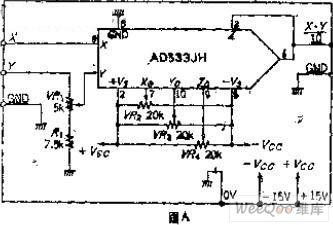
Circuit functionIn addition to be general multiplication, Analog multiplication has many other uses, such as balanced modem, synchronous detection, voltage controlled attenuator, oscillators. This circuit is a basic wiring diagram of an analog device company’s single IC multiplier AD532. Because it has been minute adjusted by the laser in-house, it can remove potentiometer that being used to adjust the X, Y input set of partial balance, just adjusts the output as long as the home side.
Circuit WorkAD532 is a differential input of the four-quadrant multiplier. It can be EO = [(X1-X2) * (Y1-Y2)] / 10 op. The input voltage range is 0 ~ +10 V, usually uses 1 / 10 scale factor.IC internal is multiplication unit composed of multiplier circuits known as Gilbert , the output impedance is low and no needs external components. The internal IC has been minute adjusted by the laser, there is no need cumbersome adjustment.The circuit only has the output offset adjustment V.AdjustmentBecause the circuit only has the offset adjustment, it only illustrates the AD533 that has not be minute adjusted.In Figure A just has one more variable resistor.It can use the basically same adjustment with the AD532.
(View)
View full Circuit Diagram | Comments | Reading(977)
single-supply,low-voltage,low-consumption operational amplifier circuit
Published:2011/5/29 7:20:00 Author:chopper | Keyword: single-supply, low-voltage, low-consumption, operational amplifier

This is a single-supply,low-voltage,low-consumption operational amplifier circuit.The operational amplifier can choose low-voltage series,such as OPA2350,MAX412,OPA2344 and so on.If the supply voltage is 5V,the resistance with * would be 42K;and if the supply voltage is 3.3V,please choose a resistance with 27K.
(View)
View full Circuit Diagram | Comments | Reading(1988)
LF347/LF147 quad operational amplifier circuit
Published:2011/5/29 7:39:00 Author:chopper | Keyword: quad operational amplifier
View full Circuit Diagram | Comments | Reading(906)
F4558 operational amplifier circuit
Published:2011/5/29 7:26:00 Author:chopper | Keyword: operational amplifier
View full Circuit Diagram | Comments | Reading(11899)
difference amplifier circuit
Published:2011/5/28 0:54:00 Author:chopper | Keyword: difference amplifier
View full Circuit Diagram | Comments | Reading(958)
LM324 four-Stage Amplifier circuit
Published:2011/5/28 0:27:00 Author:chopper | Keyword: four-Stage Amplifier


Four-Stage Amplifier circuit ,14 pins dual-in-line package filter is shown as follows.Active band-pass filter circuit is shown as follows:
Spectrum analyzer of acoustics uses this circuit as band-pass filter to select different signals from different frequency ranges,and indicates the scope of signals by using the amount of dots on a monitor lighted by LED.The circuit is shown as follows:
(View)
View full Circuit Diagram | Comments | Reading(6413)
noninverting amplifier circuit
Published:2011/5/20 5:37:00 Author:chopper | Keyword: noninverting, amplifier
View full Circuit Diagram | Comments | Reading(607)
fast inverting amplifier with high input impedance circuit
Published:2011/5/15 2:33:00 Author:John | Keyword: fast inverting amplifier

Fast inverting amplifier with high input impedance circuit is shown below.
(View)
View full Circuit Diagram | Comments | Reading(1158)
precise diode circuit
Published:2011/5/15 6:19:00 Author:chopper | Keyword: precise diode
View full Circuit Diagram | Comments | Reading(704)
Four Line Light Control Circuit
Published:2011/5/17 8:20:00 Author:Robert | Keyword: Four Line, Light, Control

The Four Line Light Control Circuit is shown below.
(View)
View full Circuit Diagram | Comments | Reading(694)
bridge amplifier circuit
Published:2011/5/16 3:12:00 Author:chopper | Keyword: bridge amplifier
View full Circuit Diagram | Comments | Reading(680)
exact clamper circuit
Published:2011/5/15 6:18:00 Author:chopper | Keyword: exact clamper
View full Circuit Diagram | Comments | Reading(1043)
| Pages:3/5 12345 |
Circuit Categories
power supply circuit
Amplifier Circuit
Basic Circuit
LED and Light Circuit
Sensor Circuit
Signal Processing
Electrical Equipment Circuit
Control Circuit
Remote Control Circuit
A/D-D/A Converter Circuit
Audio Circuit
Measuring and Test Circuit
Communication Circuit
Computer-Related Circuit
555 Circuit
Automotive Circuit
Repairing Circuit


