
Digital Circuit
Index 4
_HIGH_Q_NOTCH_FILTER
Published:2009/7/8 22:10:00 Author:May


This circuit shows a twin-T network connected to an LM102 to form a high-Q, 60-Hz notch filter. The junction of R3 and C3 which is normally connected to ground, is bootstrapped to the output of the follower.Because the output of the follower is a very low impedance, neither the depth nor the frequency of the notch change ; however, the Q is raised in proportion to the amount of signal fed back to R3 and C3. Shown is the response of a normal twin-T and the response with the follower added.
(View)
View full Circuit Diagram | Comments | Reading(889)
DIGITAL_THERMOMETER_
Published:2009/7/8 5:49:00 Author:May
Diode D2 serves assensor for driving A/D converter directly,eliminating temperature-drift er o rs normally asso-ciated with amplifiers. Can be calibrated over temperature range of -199°to 199° in either Fahrenheit or Celsius scales. Aceuracy is about 1°-H Wurzburg and M Hadley,Digital Thor-mometer Circumvents Drift,Electronics.Jan 5,1978,p 176-177
(View)
View full Circuit Diagram | Comments | Reading(1557)
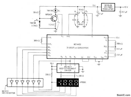
TEMPERATURE_REPORTING_DIGITAL_THERMOMETER
Published:2009/7/8 1:42:00 Author:May

The ROMs or PROMs must have the correct code for converting the data from the NE5037-used as address for the ROMs or PROMs-to the appropriate segment driver codes. The displayed amount could easily be converted to degrees Fahrenheit, °F, by the controller of (0 - 63 °temperature sensor) or through the (P) ROMs. When doing this, a third (hundreds) digit (P)ROM and display will be needed for displaying temperatures above 99 °F. An expensive clock can be made from NAND gates or inverters as shown. (View)
View full Circuit Diagram | Comments | Reading(1112)
FOUR_QUADRANT_8_BIT
Published:2009/7/7 23:06:00 Author:May

Requires only three Precision Monolithics DAC-08D/A converters to provide high-speed multiplication of two 8-bit digital words and give analog output.-J Schoeff and D. Soderquist, Differential and Multiplying Digital to Analog Converter Applications, Precision Monolithics, Santa Clara.CA,1976,AN-19,p7. (View)
View full Circuit Diagram | Comments | Reading(595)
DIGITAL_FOURIER
Published:2009/7/6 21:34:00 Author:May

Sine-wave generator produces Walsh-function approximation of sine function. Frequency of sine wave is set by square-wave input to pin 14 of 7493. Filter com ponents of opamp help smooth staircase wave form generated by summing Walsh-function components as weighted by resistors. Circuit is converter consisting of digital expander that expands input square wave into variety of digital waveforms and analog combiner that adds these waveforms to produce periodic analog output. Negative signs of Walsh harmonics are handled with digital inverter, and magnitudes are handled by choice of resistor value in summing junction. Signs and magnitudes are under microprocessor control. Net output is stairstep approximation to desired output, which can be smoothed by low-pass filter.-B. F. Jacoby, Walsh Functions: A Digital Fourier Series, BYTE, Sept. 1977, p 190-198. (View)
View full Circuit Diagram | Comments | Reading(2437)
LATCH_MEMORY
Published:2009/7/3 4:18:00 Author:May
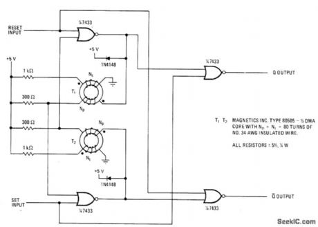
Use of saturable transformers makes memory nonvolatile and immune to false command signals. Transformers stay magnetically biased without voltage supply to provide reference state to which memory latch retumswhen power is reapplied. When bit is initially stored in circuit, set or reset pulse must have minimum width of 35 μs and minimum separation of 65 μs.-G. E. Bloom, Saturable Core Transformers Harden Latch Memories, Electronics, March 31, 1977, p 104-105. (View)
View full Circuit Diagram | Comments | Reading(783)
DIGI_TACH
Published:2009/7/3 3:40:00 Author:May
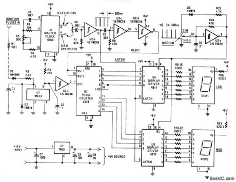
The Digi-Tach contains a master-clock circuits (U6), latch and reset pulse generators (U2-b-U2-d), input signal conditioner (U1, U2-a), pulse counter (U3), display and display drivers (DIS1, DIS2, U4, and U5), and a voltage regulator (U7). As an added feature, Digi-Tach contains a dimmer circuit (U2-e). (View)
View full Circuit Diagram | Comments | Reading(1634)
AND_LOGIC_FOR_MUTlNG
Published:2009/7/2 3:53:00 Author:May
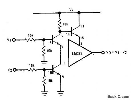
Connection shown for National LM389 combination of three transistors with opamp gives standard AND circuit for controlling muting transistor in audio sys tem. Shorting pin 12 of opamp to ground gives NAND Iogic.- Audio Handbook, National Semiconductor, Santa Clara, CA, 1977, p 4-33-4-37. (View)
View full Circuit Diagram | Comments | Reading(607)
LATCH
Published:2009/7/2 3:51:00 Author:May
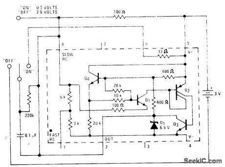
National LM3909 IC operating from 3-V battery requires only momentary contact by switch to change logic level of output and hold that level.- Linear Applications.Vol, 2, National Semiconductor, Santa Clara,CA,1976,AN-154,p9 (View)
View full Circuit Diagram | Comments | Reading(606)
HIGH_INPUT_IMPEDANCE
Published:2009/6/28 23:43:00 Author:May

Use of JFET as isolator boosts input impedance of opamp to 22 megohms for low-frequency input signals.Impedance drops to 3.9 megohms as frequency increases to about 20 kHz. Overall gain of circuit is about 45 dB when using 18-V supply.- Audio Handbook, National Semiconductor, Santa Clara, CA, 1977, p 4-21-4-28. (View)
View full Circuit Diagram | Comments | Reading(0)
74 Series digital circuit of 74LS363 octal D flip-flop(tristate)
Published:2011/7/25 3:48:00 Author:Lucas | Keyword: 74 Series , digital circuit , octal D flip-flop, tristate

Edge-triggered D flip-flop; the minimum Voh level is 3.65V; 74LS374 is similar with the circuit, but the typical minimum VOH is 2.4V.
Q0 = the output level before establishing the steady-state input conditions.
(View)
View full Circuit Diagram | Comments | Reading(771)
74 Series digital circuit of 74LS364 octal D flip-flop(tristate)
Published:2011/7/25 3:45:00 Author:Lucas | Keyword: 74 Series, digital circuit , octal D flip-flop, tristate


Q0 = the output level before establishing the steady-state input conditions.
Edge-triggered D flip-flop; the minimum Voh level is 3.65V; 74LS374 is similar with the circuit, but the typical minimum VOH is 2.4V.
(View)
View full Circuit Diagram | Comments | Reading(677)
74 Series digital circuit of 74365A/366A six buffer / bus driver(three-state)
Published:2011/8/1 1:22:00 Author:Lucas | Keyword: 74 Series , digital circuit , six buffer , bus driver, three-state

Three-state output; 365 is the in-phase output; 366 is the inverted output; G1 and G2 are the public control.
(View)
View full Circuit Diagram | Comments | Reading(609)
74 Series digital circuit of 74367A/368A six buffer / bus driver
Published:2011/8/1 1:20:00 Author:Lucas | Keyword: 74 Series, digital circuit, six buffer , bus driver

Three-state output; 367 is the in-phase output; 368 is the inverted output; G1 non-controls four doors (1 ~ 4), and G2 non-controls the other two doors.
(View)
View full Circuit Diagram | Comments | Reading(760)
2_W_WITH_IC
Published:2009/6/28 23:26:00 Author:May


Uses Motorola MFC9020 audio power amplifier to give maximum output of about 2 W for 16-ohm loudspeaker. Used in autopatch system for FM repeaten-R. B. Shreve, A Versatile Autopatch System for VHF FM Repeaters, Ham Radio, July 1974, p 32-38. (View)
View full Circuit Diagram | Comments | Reading(1)
74 Series digital circuit of 74LS374 octal D flip-flop(tristate)
Published:2011/7/25 3:31:00 Author:Lucas | Keyword: 74 Series , digital circuit , octal D flip-flop, tristate

Three-state output: all the load is full parallel stored; it has buffer control input; clock pulse positive edge is triggered; 74LS364 is the similar to 74LS374 but has the MOS interface, high VOH.
Q0 = the output level before establishing the steady-state input conditions.
(View)
View full Circuit Diagram | Comments | Reading(2034)
70_dB_GAIN_WITH_15_V
Published:2009/6/28 23:24:00 Author:May

Operates from sihgle penlight qell at current drain of 0.5 mA. ldeal as self-contained unit inserted in microphone cable. Q2-Q4 form 70-dB voltage amplifier. Q5 is detector, and Q6 is emitter-follower driving AGC transistor Q1.3-dB bandwidth is about 100 Hz to 8 kHz. Full output is about 200 mVRMS, while low output terminal is 1 mVRMS.-C.Hall, Low-Voltage Audio AGO Amplifier, Ham Radio, Dec. 1973, p 32-34. (View)
View full Circuit Diagram | Comments | Reading(3095)
74 Series digital circuit of 74LS385, 74F385 four serial adder / subtractor
Published:2011/8/1 1:15:00 Author:Lucas | Keyword: 74 Series , digital circuit , four serial adder , subtractor

It has buffered clock and direct clear input; 2's complement independent add/ subtract and four independent outputs are related to A and B inputs controlled by S / A console.
(View)
View full Circuit Diagram | Comments | Reading(1315)
74 Series digital circuit of 74S412 multi-mode buffer latch (tristate)
Published:2011/7/25 3:25:00 Author:Lucas | Keyword: 74 Series , digital circuit , multi-mode buffer latch , tristate

Three-state output; mode input or selecting input allows output to storage in the enabled or disabled state; the typical value of high output is 4V, which can directly drive most of the MOS circuit; it can exchange with Intel 312 or 8212 directly.
Q0 = the output level before establishing the steady-state input conditions.
(View)
View full Circuit Diagram | Comments | Reading(928)
74 Series digital circuit of 74LS423, 74HC423 dual retriggerable monostable multivibrator (with clearing)
Published:2011/7/25 3:39:00 Author:Lucas | Keyword: 74 Series, digital circuit , dual retriggerable , monostable multivibrator , clearing

Two oscillators have a negative trigger input A and a positive trigger input B, but each end can be used to ban on the importation; when the clearing input end is in single-pulse low level, it is enable to clear, but will not be cleared trigger.
*is the unstable state.
(View)
View full Circuit Diagram | Comments | Reading(769)
| Pages:4/19 12345678910111213141516171819 |
Circuit Categories
power supply circuit
Amplifier Circuit
Basic Circuit
LED and Light Circuit
Sensor Circuit
Signal Processing
Electrical Equipment Circuit
Control Circuit
Remote Control Circuit
A/D-D/A Converter Circuit
Audio Circuit
Measuring and Test Circuit
Communication Circuit
Computer-Related Circuit
555 Circuit
Automotive Circuit
Repairing Circuit